ALLPCB


In the fast-paced world of portable gaming devices, ensuring top-notch performance is key. One critical factor that can make or break the user experience is signal integrity in the printed circuit boards (PCBs) that power these devices. If you're searching for ways to enhance signal integrity PCB gaming console designs, you're in the right place. This blog will guide you through practical strategies like impedance control PCB design gaming, high-speed routing techniques PCB, EMI reduction strategies gaming PCB, and signal layer stackup optimization to achieve flawless performance in your gaming hardware.
Whether you're a hardware engineer or a designer working on the next big portable gaming gadget, this comprehensive guide will walk you through the essentials of maintaining signal quality, reducing noise, and optimizing your PCB layout for high-speed data transfer. Let's dive into the details of creating reliable and efficient gaming device PCBs.
Why Signal Integrity Matters in Portable Gaming Devices
Portable gaming devices, like handheld consoles, rely on high-speed data transfer to deliver smooth graphics, quick response times, and seamless multiplayer connectivity. Signal integrity refers to the ability of electrical signals to travel through a PCB without distortion or interference. When signal integrity is compromised, you might face issues like data loss, lag, or even system crashes—problems no gamer wants to deal with.
In high-speed designs, signals can degrade due to factors like crosstalk, electromagnetic interference (EMI), or improper impedance matching. For gaming devices with compact designs, where space is limited, maintaining signal integrity becomes even more challenging. That's why optimizing your PCB design for signal integrity PCB gaming console applications is crucial for delivering a reliable and immersive gaming experience.
Key Challenges in High-Speed PCB Design for Gaming Devices
Before diving into solutions, it's important to understand the specific challenges that affect signal integrity in portable gaming device PCBs. These devices often operate at high frequencies, sometimes exceeding 1 GHz for data transfer between components like GPUs, memory, and display controllers. Here are some common issues:
- Compact Layouts: Limited space means traces are closer together, increasing the risk of crosstalk and noise.
- High-Speed Signals: Faster data rates (e.g., 5 Gbps or more for modern interfaces) make signals more susceptible to reflections and timing errors.
- Power Constraints: Portable devices rely on batteries, so power delivery must be efficient to avoid noise in the system.
- EMI Sensitivity: External and internal interference can disrupt signal quality, especially in densely packed designs.
Addressing these challenges requires a combination of careful planning, precise design techniques, and an understanding of signal behavior. Let's explore actionable strategies to optimize your PCB for gaming applications.
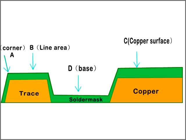
Impedance Control in PCB Design for Gaming Devices
One of the cornerstones of maintaining signal integrity is impedance control PCB design gaming. Impedance is the resistance a signal faces as it travels along a trace. If the impedance isn't consistent, signals can reflect back, causing distortions or delays. For high-speed interfaces like USB-C or HDMI used in gaming devices, maintaining a specific impedance (often 50 ohms for single-ended signals or 100 ohms for differential pairs) is critical.
To achieve proper impedance control, consider the following:
- Trace Width and Spacing: Use PCB design tools to calculate the trace width and spacing needed for your target impedance. For example, a 50-ohm trace on a standard FR-4 material might require a width of around 6 mils with a specific dielectric thickness.
- Dielectric Material: Choose materials with a consistent dielectric constant (Dk) to avoid impedance variations. FR-4 is common, but for higher frequencies, consider low-loss materials.
- Reference Planes: Ensure continuous ground or power planes beneath signal traces to provide a stable return path and maintain impedance.
By prioritizing impedance control, you can minimize signal reflections and ensure data integrity, which is essential for lag-free gaming performance.
High-Speed Routing Techniques for Gaming PCBs
Routing high-speed signals on a PCB is like directing traffic on a busy highway—any wrong turn or congestion can cause delays or crashes. Using effective high-speed routing techniques PCB is vital to prevent signal degradation in gaming devices. Here are some proven routing strategies:
- Minimize Trace Lengths: Keep high-speed traces as short as possible to reduce signal delay and attenuation. For instance, DDR memory lines in gaming consoles should be routed with matched lengths to avoid timing mismatches.
- Avoid Sharp Corners: Use 45-degree angles or curved traces instead of 90-degree bends to prevent signal reflections.
- Differential Pair Routing: For interfaces like USB or PCIe, route differential pairs with equal lengths and consistent spacing to maintain signal balance.
- Via Management: Minimize the use of vias for high-speed signals, as they can introduce impedance discontinuities. If vias are necessary, use back-drilling to remove unused via stubs.
These routing techniques help ensure that signals reach their destination without interference, supporting the high data rates required for modern gaming hardware.

EMI Reduction Strategies for Gaming PCBs
Electromagnetic interference (EMI) can wreak havoc on signal integrity, leading to glitches or dropped connections in gaming devices. Implementing EMI reduction strategies gaming PCB is essential to create a stable environment for high-speed signals. Here are some effective approaches:
- Ground Planes: Use solid ground planes to shield signals from external noise and provide a low-impedance return path. Avoid splitting ground planes under high-speed traces.
- Decoupling Capacitors: Place decoupling capacitors (e.g., 0.1 μF) near power pins of ICs to filter out high-frequency noise from the power supply.
- Shielding: In compact gaming devices, consider adding metal shields over sensitive components to block external EMI.
- Trace Spacing: Increase spacing between high-speed traces to reduce crosstalk, a common source of EMI in dense layouts.
By focusing on these strategies, you can significantly reduce EMI, ensuring that your gaming device operates smoothly even in noisy environments.
Signal Layer Stackup Optimization for Gaming Devices
The way you stack the layers of your PCB plays a huge role in signal integrity. Signal layer stackup optimization involves arranging signal, ground, and power layers to minimize noise and support high-speed performance. For portable gaming devices, where board thickness is often limited to 1.6 mm or less, a well-designed stackup is even more important.
Consider these tips for optimizing your PCB stackup:
- Symmetrical Stackup: Use a balanced layer arrangement (e.g., 4-layer or 6-layer boards) to prevent warping and ensure signal stability. A typical 4-layer stackup might be Signal-Ground-Power-Signal.
- Ground Layer Proximity: Place ground layers adjacent to high-speed signal layers to provide a consistent return path and reduce loop inductance.
- Power Distribution: Dedicate internal layers for power distribution to minimize voltage drops and noise in the system.
- Layer Count: For complex gaming designs with multiple high-speed interfaces, consider 6 or 8 layers to segregate signals and reduce interference.
A well-optimized stackup not only improves signal integrity but also enhances the overall durability and performance of the PCB in a compact gaming device.
Practical Tips for Testing and Validation
Designing a PCB with optimal signal integrity is only half the battle. Testing and validation are crucial to ensure your design performs as expected in real-world conditions. Here are some practical steps to verify your gaming device PCB:
- Time-Domain Reflectometry (TDR): Use TDR to measure impedance along traces and identify discontinuities or mismatches.
- Eye Diagram Analysis: Evaluate signal quality using eye diagrams to check for jitter, noise, and timing issues at high data rates (e.g., 5 Gbps).
- EMI Testing: Conduct radiated and conducted EMI tests to ensure compliance with standards like FCC or CE for consumer electronics.
- Simulation Tools: Leverage PCB simulation software to predict signal behavior and identify potential issues before fabrication.
Regular testing helps catch problems early, saving time and costs during the development of your gaming device.
Conclusion: Building Better Gaming Devices with Optimized PCBs
Optimizing signal integrity in high-speed portable gaming device PCBs is a multi-faceted process that requires attention to detail and a deep understanding of design principles. By focusing on impedance control PCB design gaming, employing high-speed routing techniques PCB, implementing EMI reduction strategies gaming PCB, and prioritizing signal layer stackup optimization, you can create reliable, high-performance hardware that meets the demands of modern gamers.
At ALLPCB, we’re committed to supporting engineers and designers in bringing their innovative gaming devices to life. With the right design practices and manufacturing expertise, you can ensure your signal integrity PCB gaming console projects deliver exceptional performance in every handheld unit. Start applying these strategies today to build gaming hardware that stands out in a competitive market.