 ALLPCB


In the fast-evolving world of edge computing, creating compact PCB designs is crucial for fitting powerful technology into small, space-constrained applications. Whether it’s for IoT devices, wearable tech, or industrial sensors, the demand for smaller, efficient printed circuit boards (PCBs) continues to grow. This blog dives deep into proven techniques for miniaturizing edge computing PCBs, focusing on compact PCB design for edge computing, miniaturization techniques for PCBs, HDI PCB solutions for edge computing, component placement optimization, and via selection for small PCBs. Let’s explore how to achieve high performance in tiny spaces with practical tips and detailed insights.
Why Miniaturization Matters in Edge Computing PCBs
Edge computing brings data processing closer to the source, reducing latency and improving real-time decision-making. However, devices used in edge computing often operate in tight spaces, like smart home gadgets or automotive systems. Miniaturizing PCBs allows engineers to pack more functionality into smaller footprints without sacrificing performance. The challenge lies in balancing size, power efficiency, and signal integrity while meeting the demands of high-speed data processing.
Miniaturization isn’t just about making things smaller—it’s about smarter design. By using advanced techniques, you can reduce the physical size of a PCB while maintaining or even enhancing its capabilities. Let’s break down the key strategies to achieve this for edge computing applications.
Key Techniques for Compact PCB Design in Edge Computing
Creating a compact PCB design for edge computing requires a combination of innovative technologies and careful planning. Below are the most effective approaches to achieve miniaturization without compromising functionality.
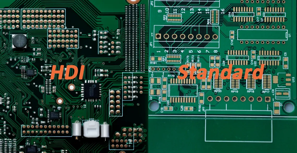
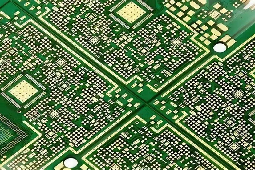
1. Leveraging High-Density Interconnect (HDI) PCB Technology
High-Density Interconnect (HDI) PCB technology is a game-changer for miniaturization in edge computing. HDI PCBs use finer lines, smaller vias, and denser component layouts to fit more circuitry into a smaller area. This is especially useful for edge devices that require high-speed data transfer and complex processing.
Key features of HDI PCBs include:
- Microvias: These tiny vias (often less than 0.15 mm in diameter) connect layers in a PCB, allowing for denser routing and reduced board size.
- Finer Traces: HDI boards often have trace widths as small as 0.075 mm, compared to 0.2 mm on standard PCBs, enabling more connections in less space.
- Layer Stacking: By stacking multiple layers with precise alignment, HDI PCBs increase functionality without expanding the board’s footprint.
For edge computing, HDI PCB technology ensures that devices like smart cameras or industrial IoT sensors can handle high data rates (often exceeding 5 Gbps) while fitting into compact enclosures. The use of HDI also improves signal integrity by reducing noise and crosstalk, which is critical for maintaining performance in small designs.
2. Miniaturization Techniques for PCB Layouts
Beyond HDI technology, several miniaturization techniques for PCBs can help engineers shrink designs for edge computing applications. These methods focus on optimizing every aspect of the board’s layout.
- Use Smaller Components: Opt for surface-mount devices (SMDs) with smaller packages, such as 0201 or 01005 resistors and capacitors. These components take up less space than traditional through-hole parts.
- Double-Sided Assembly: Place components on both sides of the PCB to maximize the use of available space. This is particularly effective for compact designs in wearable edge devices.
- Reduce Board Layers Where Possible: While HDI often involves more layers, careful planning can sometimes reduce the layer count by optimizing routing, saving space and cost.
By applying these miniaturization techniques, a PCB for an edge computing device can shrink from a typical 50 mm x 50 mm footprint to as small as 20 mm x 20 mm, depending on the application. This reduction is vital for fitting into constrained spaces like medical implants or compact drones.
3. Component Placement Optimization for Edge Computing
Component placement optimization is a critical step in designing compact PCBs for edge computing. Poor placement can lead to signal interference, heat buildup, and wasted space. Here’s how to get it right:
- Group Related Components: Place components that interact frequently, like a microcontroller and its supporting capacitors, close together to minimize trace lengths and reduce latency.
- Prioritize High-Speed Components: Position high-speed components, such as processors for edge data processing, near the center or away from noisy areas to maintain signal integrity at speeds up to 10 Gbps.
- Manage Thermal Distribution: Spread out heat-generating components to avoid hotspots. For example, place power regulators away from sensitive analog circuits to prevent thermal interference.
Effective component placement can reduce signal delays by up to 20% and improve the overall reliability of edge computing devices, especially in harsh environments like industrial settings.
4. Via Selection for Small PCBs
Vias are the tiny holes that connect different layers of a PCB, and choosing the right type is essential for miniaturization in small PCBs. For edge computing designs, where space is limited, via selection can significantly impact the board’s size and performance.
- Blind Vias: These connect an outer layer to an inner layer without going through the entire board, saving space on the opposite side. They’re ideal for HDI designs in edge devices.
- Buried Vias: These connect inner layers only, staying hidden from the surface. They allow for denser routing without increasing the board’s footprint.
- Microvias: As mentioned earlier, microvias are smaller (often 0.1 mm or less) and laser-drilled, enabling high-density connections in compact PCBs.
Using microvias instead of traditional through-hole vias can reduce via diameter by up to 50%, freeing up space for additional traces or components. However, microvias require precise manufacturing to ensure reliability, especially for high-speed signals in edge computing applications where impedance mismatches can cause data errors.
Challenges in Miniaturizing Edge Computing PCBs
While miniaturization offers many benefits, it also comes with challenges that engineers must address to ensure performance and reliability in edge computing devices.
- Signal Integrity Issues: As traces and components get closer together, the risk of crosstalk and electromagnetic interference (EMI) increases. Maintaining impedance control (often around 50 ohms for high-speed signals) becomes critical.
- Thermal Management: Smaller boards have less surface area to dissipate heat. High-performance edge computing chips can generate significant heat, requiring careful design to avoid overheating.
- Manufacturing Complexity: Techniques like HDI and microvias demand advanced fabrication processes, which can increase costs and require tight tolerances (e.g., alignment accuracy within 0.05 mm).
To overcome these challenges, simulation tools can predict signal behavior and thermal performance before manufacturing. For instance, maintaining a ground plane near high-speed traces can reduce EMI by up to 30%, ensuring reliable operation in compact designs.
Practical Applications of Compact PCB Designs in Edge Computing
Compact PCB designs are transforming edge computing across various industries. Here are a few real-world examples where miniaturization plays a vital role:
- Smart Wearables: Devices like fitness trackers rely on tiny PCBs to process sensor data locally, using HDI technology to fit into wristband-sized enclosures.
- Industrial IoT: Sensors in factories use miniaturized PCBs to monitor equipment in real-time, fitting into small control units with limited space.
- Automotive Systems: Edge computing modules in vehicles process data from cameras and sensors for autonomous driving, requiring compact designs to integrate into dashboards or engine compartments.
In each of these cases, techniques like HDI PCB design, component placement optimization, and via selection enable powerful computing in incredibly small spaces, driving innovation in edge technology.
Tips for Designing Compact PCBs for Edge Computing
If you’re embarking on a project involving compact PCB design for edge computing, consider these actionable tips to ensure success:
- Start with a clear understanding of the space constraints and performance requirements of your application.
- Use design software to simulate signal integrity and thermal performance before finalizing the layout.
- Collaborate with manufacturing partners early to confirm the feasibility of HDI features like microvias and fine traces.
- Test prototypes under real-world conditions to identify potential issues with heat or interference.
By following these steps, you can create reliable, high-performing PCBs that meet the unique demands of edge computing in space-constrained environments.
Conclusion: The Future of Miniaturization in Edge Computing PCBs
Miniaturizing edge computing PCBs is no longer just an option—it’s a necessity for staying competitive in today’s tech-driven world. By adopting techniques like HDI PCB technology, optimizing component placement, and selecting the right vias for small PCBs, engineers can create compact designs that deliver exceptional performance. These strategies not only save space but also enhance signal integrity and power efficiency, making them ideal for applications ranging from wearables to industrial systems.
As technology continues to advance, the push for smaller, smarter devices will only intensify. Staying ahead means mastering the art of miniaturization with innovative design practices and precise manufacturing. With the right approach, compact PCB design for edge computing can unlock endless possibilities for space-constrained applications.


