 ALLPCB


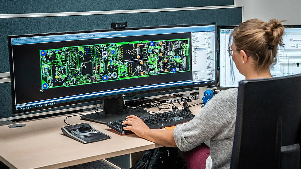
As an electronics engineering student, mastering PCB design is a crucial step in transitioning from classroom projects to a successful career. Whether you're working on a simple circuit or a complex system, understanding advanced PCB layout techniques can set you apart. In this comprehensive guide, we'll explore key concepts like signal integrity in student PCB projects, power integrity in student PCB designs, high-speed PCB design education, and EMI mitigation in educational PCBs. Let’s dive into actionable strategies to elevate your skills and prepare for real-world challenges with advanced PCB layout techniques for students.
Why PCB Design Skills Matter for Students
PCB design is the backbone of modern electronics. Every device, from smartphones to medical equipment, relies on well-designed printed circuit boards. For students, learning these skills early offers a competitive edge in internships, projects, and future job applications. By focusing on advanced techniques, you can tackle complex designs, minimize errors, and create efficient, reliable circuits. This blog will break down essential topics to help you build a strong foundation and stand out in the field.
1. Mastering Advanced PCB Layout Techniques for Students
Creating an effective PCB layout goes beyond placing components and connecting traces. Advanced PCB layout techniques for students involve optimizing space, ensuring functionality, and preparing for manufacturing. Here are some key strategies to focus on:
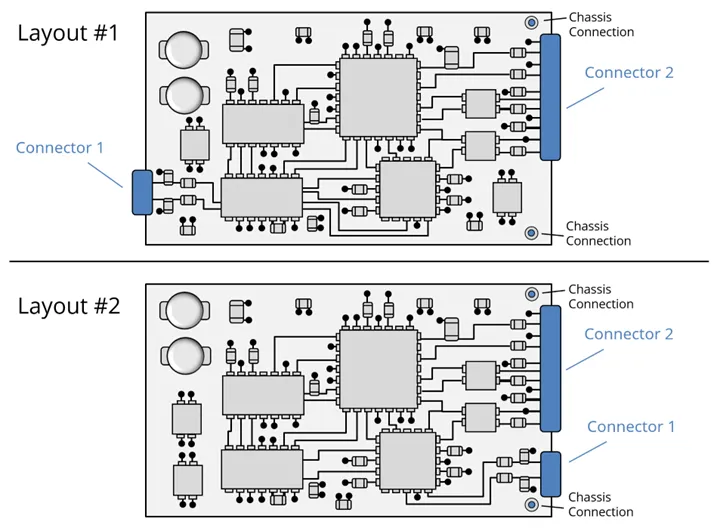
- Component Placement: Start by grouping related components together to minimize trace lengths. For example, place decoupling capacitors close to power pins of ICs (within 0.1 inches or 2.54 mm) to reduce noise.
- Trace Routing: Avoid sharp 90-degree angles in traces, as they can cause signal reflection. Use 45-degree angles or curves for smoother signal flow.
- Layer Management: For multi-layer boards, dedicate specific layers to power and ground planes. This reduces interference and improves signal stability.
By practicing these techniques in your classroom projects, you’ll develop habits that translate directly to professional designs. Start with small circuits and gradually work on more complex layouts to build confidence.
2. Ensuring Signal Integrity in Student PCB Projects
Signal integrity refers to the quality of electrical signals as they travel through your PCB. Poor signal integrity in student PCB projects can lead to data loss, delays, or complete circuit failure. Here’s how to maintain clean signals:
- Controlled Impedance: For high-speed signals (above 50 MHz), match the trace impedance to the source and load. A common target is 50 ohms for single-ended signals. Use online calculators or design tools to determine trace width and spacing.
- Minimize Crosstalk: Keep high-speed traces at least 3 times the trace width apart to prevent interference. For example, if your trace is 5 mils wide, maintain a 15-mil gap.
- Proper Termination: Use resistors or other termination techniques to prevent signal reflections at the end of long traces.
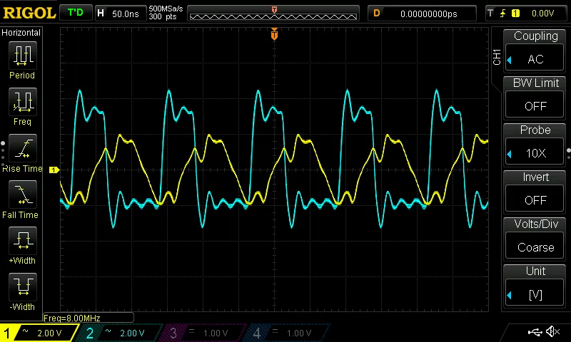
Signal integrity issues are common in student projects due to limited experience with high-speed designs. Test your circuits with an oscilloscope to spot distortions and adjust your layout accordingly. This hands-on approach builds critical troubleshooting skills.
3. Focusing on Power Integrity in Student PCB Designs
Power integrity ensures that your circuit receives stable voltage and current without fluctuations. In student PCB designs, power integrity issues can cause unexpected behavior or component damage. Follow these tips to maintain a robust power delivery network:
- Decoupling Capacitors: Place capacitors (e.g., 0.1 μF ceramic) near every power pin of active components to filter noise. Ensure the capacitor’s lead length is under 0.2 inches (5 mm) for best results.
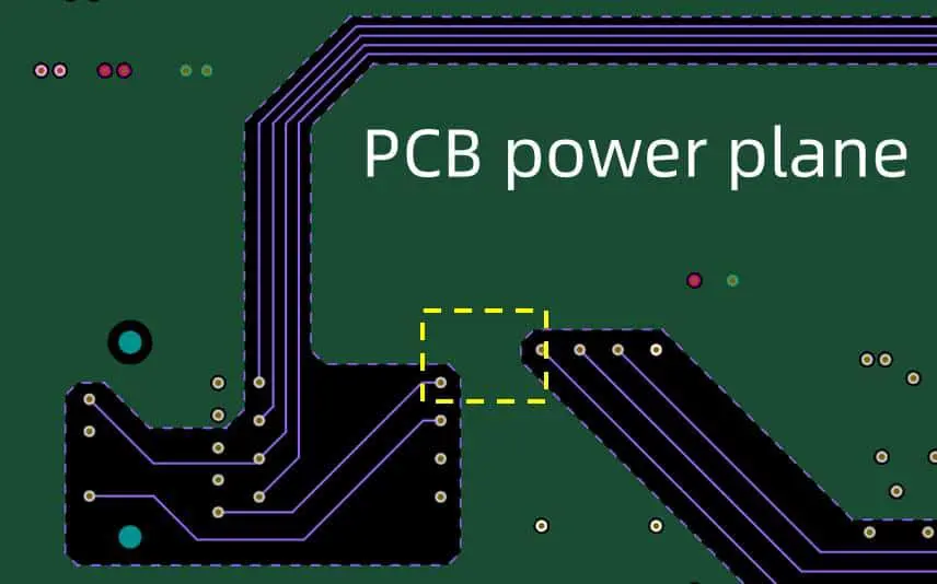
- Power Planes: Use dedicated power and ground planes in multi-layer boards to provide low-impedance paths. This reduces voltage drops across the board.
- Wider Traces for Power: Design power traces wider than signal traces (e.g., 20-30 mils for 1A current) to handle higher currents without overheating.
Power integrity is often overlooked in educational projects, but it’s a critical skill for professional designs. Simulate your power distribution network using design software to identify weak points before fabrication.
4. Learning High-Speed PCB Design Education
High-speed PCB design education is essential for students working on modern electronics, where signals often exceed 100 MHz. These designs require careful attention to timing, impedance, and interference. Here are key concepts to study:
- Signal Propagation Delay: At high speeds, signals take time to travel along traces. For instance, a signal on a standard FR4 board travels at about 6 inches per nanosecond. Keep traces short to avoid timing issues.
- Differential Pairs: For high-speed data (like USB or HDMI), use differential pairs with equal trace lengths to maintain signal synchronization.
- Stack-Up Design: Plan your board stack-up to include ground planes adjacent to signal layers. This shields signals and controls impedance.
Many universities and online platforms offer courses on high-speed design. Supplement your curriculum with practical projects, such as designing a simple USB interface, to apply these principles. Hands-on experience in high-speed PCB design education prepares you for industry demands.
5. Implementing EMI Mitigation in Educational PCBs
Electromagnetic interference (EMI) can disrupt your circuit’s performance or interfere with nearby devices. EMI mitigation in educational PCBs is a valuable skill that ensures compliance with regulatory standards. Use these techniques to reduce EMI:
- Grounding: Create a solid ground plane to provide a low-impedance return path for currents. Avoid splitting the ground plane unless absolutely necessary.
- Shielding: Enclose sensitive components in metal shields or use guard traces around high-frequency signals to block interference.
- Trace Spacing: Maintain adequate spacing between traces (e.g., 10 mils for low-speed signals, more for high-speed) to prevent coupling and radiation.
EMI issues are challenging to diagnose without specialized equipment, but you can minimize risks by following best practices from the start. Test your designs in different environments to see how external noise affects performance, and adjust your layout as needed.
Tools and Resources for PCB Design Learning
As a student, access to the right tools can accelerate your learning. Many free or student-friendly software options allow you to practice advanced PCB layout techniques. Look for programs that offer simulation features to test signal and power integrity. Additionally, online tutorials, forums, and university libraries often provide guides on high-speed design and EMI mitigation.
Experiment with different tools to find what suits your workflow. Some platforms also offer free or discounted PCB fabrication for students, allowing you to test your designs in real life. Take advantage of these opportunities to iterate and improve.
Bridging the Gap: From Classroom to Career
Transitioning from academic projects to a professional career requires more than technical skills. Here’s how to apply what you’ve learned about PCB design in the real world:
- Build a Portfolio: Document your projects, highlighting challenges like signal integrity or EMI mitigation. Showcase how you solved these issues with specific data (e.g., reduced noise by 30% with proper grounding).
- Internships: Seek internships where you can work on real PCB designs. Hands-on experience with industry-standard tools and processes is invaluable.
- Stay Updated: Electronics evolve rapidly. Follow industry blogs, webinars, and research papers to keep up with trends in high-speed design and power integrity.
Your classroom projects are the foundation, but continuous learning and practical application will define your career. Focus on mastering advanced techniques now to stand out as a skilled engineer later.
Common Mistakes to Avoid in Student PCB Designs
Even with the best intentions, students often make mistakes that can derail a project. Here are pitfalls to watch out for:
- Ignoring Design Rules: Always check design rules for trace width, spacing, and via sizes. Violating these can lead to manufacturing errors.
- Overloading Power Traces: Underestimating current needs can cause traces to overheat. Use calculators to determine appropriate widths.
- Neglecting Testing: Don’t assume your design works without testing. Use multimeters and oscilloscopes to verify signal and power integrity.
Learning from mistakes is part of the process. Keep a record of issues you encounter and how you resolved them to avoid repeating errors in future designs.
Conclusion: Elevate Your PCB Design Skills Today
As an electronics engineering student, diving into advanced PCB layout techniques for students opens doors to exciting career opportunities. By focusing on signal integrity in student PCB projects, power integrity in student PCB designs, high-speed PCB design education, and EMI mitigation in educational PCBs, you’re building skills that employers value. Start small, practice consistently, and use every project as a chance to learn. With dedication, you’ll transform from a classroom learner to a confident professional ready to tackle complex designs.
Take the first step today by applying these techniques in your next project. The journey from classroom to career begins with a single circuit, and every design brings you closer to mastery.


