 ALLPCB


In the fast-evolving world of electronics, flexible semiconductor PCBs are becoming a game-changer, especially in wearable technology. If you're wondering how flexible PCB design works or what role it plays in wearable electronics PCB applications, this guide is for you. We'll explore the essentials of designing flexible PCBs, the materials used, and their transformative impact on devices like smartwatches and fitness trackers. From understanding flex PCB materials to diving into rigid-flex PCB solutions and the importance of PCB bending radius, this post covers it all with practical insights for engineers and tech enthusiasts.
Let’s dive deeper into the world of flexible PCBs and uncover how they’re shaping the future of wearable electronics with innovative designs and unmatched adaptability.
What Are Flexible Semiconductor PCBs?
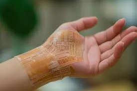
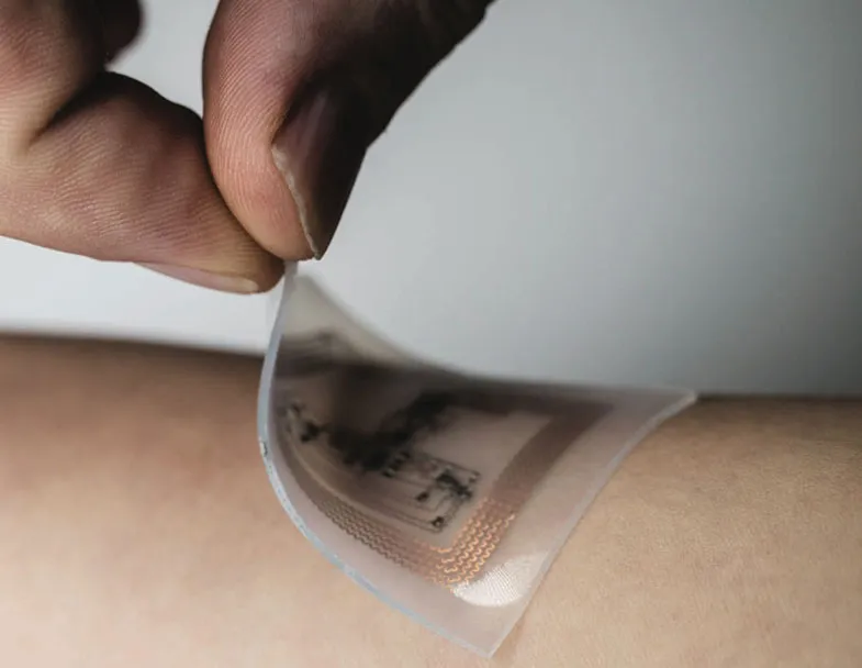
Flexible semiconductor PCBs, often called flexible printed circuit boards, are thin, lightweight circuits that can bend and fold without breaking. Unlike traditional rigid boards, these circuits are built on flexible substrates, allowing them to conform to unique shapes and fit into compact spaces. This makes them ideal for modern devices, especially in wearable electronics PCB designs where space and comfort are critical.
These PCBs are made using advanced manufacturing techniques and materials like polyimide, which provide durability even under repeated bending. Their ability to integrate with semiconductors—tiny chips that power electronic functions—further enhances their value in creating smart, connected devices. Whether it’s a heart rate sensor in a fitness band or a display driver in a foldable phone, flexible PCBs are at the core of innovation.
Why Flexible PCBs Matter in Wearable Electronics
Wearable electronics, such as smartwatches, medical patches, and augmented reality glasses, demand circuits that are not only small but also adaptable to movement and curved surfaces. Flexible PCBs meet these needs by offering:
- Space Efficiency: They can be folded or layered, reducing the overall size of the device.
- Durability: Designed to withstand millions of flex cycles—some tested up to 200,000 cycles without failure.
- Lightweight Design: Often weighing less than 1 gram per square inch, they’re perfect for wearables.
Key Elements of Flexible PCB Design
Creating a successful flexible PCB design requires careful planning and attention to detail. Engineers must consider factors like material choice, layout, and the physical stresses the board will face. Below are the critical aspects of designing these innovative circuits for wearable technology.
1. Understanding PCB Bending Radius
The PCB bending radius is a crucial factor in flexible PCB design. It refers to the tightest curve a board can make without damaging the traces or materials. A smaller bending radius allows for tighter folds, but pushing it too far can cause cracks or signal loss. Industry standards often recommend a minimum bending radius of 10 times the thickness of the board for dynamic applications (where bending happens repeatedly). For example, a 0.1 mm thick PCB should have a bending radius of at least 1 mm.
In wearable electronics, where devices are constantly moving, designers must balance flexibility with reliability. Using simulation tools to test bending stress can prevent failures during real-world use.
2. Choosing the Right Flex PCB Materials
The choice of flex PCB materials directly impacts performance and durability. Common materials include:
- Polyimide (PI): Known for high heat resistance (up to 400°C) and excellent flexibility, making it ideal for dynamic bending in wearables.
- Polyester (PET): A cost-effective option for less demanding applications, though less durable under repeated flexing.
- Copper Foils: Typically 18-35 micrometers thick, used for conductive traces due to their flexibility and conductivity.
Selecting the right material depends on the device’s requirements. For instance, a medical wearable monitoring vital signs might prioritize polyimide for its reliability under constant movement.
3. Trace Routing and Layout Considerations
In flexible PCB design, trace routing must account for bending areas. Straight traces are prone to cracking under stress, so designers often use curved or teardrop-shaped traces to distribute stress evenly. Additionally, avoiding vias (small holes for connections) in bend zones reduces the risk of damage. For high-speed signals in wearables, impedance control is vital—targeting values like 50 ohms for RF applications ensures signal integrity.
Layer stacking also plays a role. A typical flexible PCB might have 1-4 layers, with a balanced stackup to minimize warping. For example, a 2-layer design might use a 25-micrometer polyimide base with 18-micrometer copper on each side for optimal flexibility.
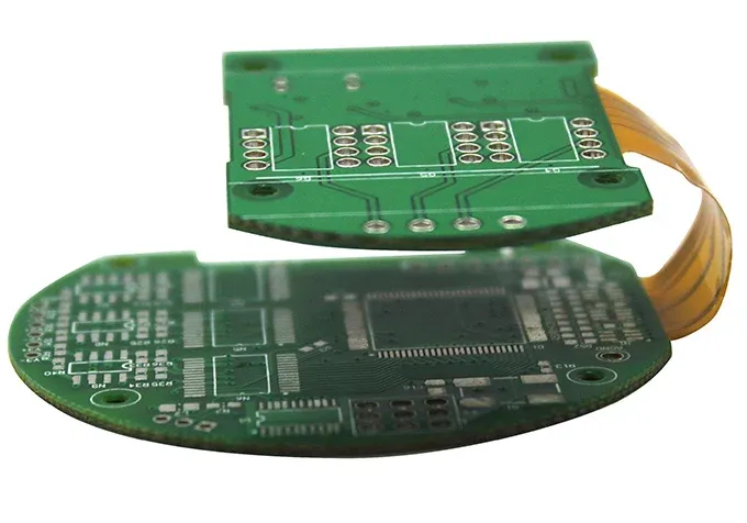
Rigid-Flex PCB: Combining Strength and Flexibility
A rigid-flex PCB combines the benefits of rigid and flexible circuits into a single board. Rigid sections provide structural support for mounting components, while flexible sections allow bending or folding. This hybrid approach is increasingly popular in wearable electronics, where devices need both durability and adaptability.
Benefits of Rigid-Flex in Wearables
Rigid-flex PCBs offer several advantages:
- Reduced Assembly Costs: Combining rigid and flexible areas eliminates the need for multiple connectors, cutting assembly time by up to 30% in some cases.
- Enhanced Reliability: Fewer connection points mean lower chances of failure, critical for wearables used in harsh conditions.
- Compact Design: Ideal for fitting into tight spaces, like the curved housing of a smart ring.
For instance, a fitness tracker might use a rigid-flex PCB to house its processor on a stable rigid section while connecting to a flexible antenna that wraps around the wristband for better signal reception.
Applications of Flexible PCBs in Wearable Electronics
The rise of wearable technology has created a massive demand for wearable electronics PCB solutions. Flexible PCBs are at the heart of many cutting-edge devices, enabling functionality that was once impossible. Here are some key applications:
1. Fitness Trackers and Smartwatches
Devices like fitness trackers rely on flexible PCBs to fit sensors, batteries, and displays into slim, comfortable designs. These boards can bend to match the curve of a wrist, ensuring a snug fit without sacrificing performance. For example, heart rate sensors often use flexible circuits to maintain contact with the skin, delivering accurate readings with signal noise below 0.1 mV.
2. Medical Wearables
In healthcare, flexible PCBs power wearable devices like glucose monitors and ECG patches. These devices need to conform to the body for continuous monitoring, often requiring a PCB bending radius as tight as 2 mm. The lightweight nature of flex PCBs—sometimes under 0.5 grams—ensures patient comfort during long-term use.
3. Augmented Reality (AR) Glasses
AR glasses use flexible PCBs to connect displays, cameras, and batteries across hinged or curved frames. The ability to route high-speed signals (up to 5 Gbps in some designs) through flexible traces ensures seamless data transfer without bulky wiring.
Challenges in Flexible PCB Design for Wearables
While flexible PCBs offer incredible benefits, they come with unique challenges that engineers must address during design and manufacturing.
1. Managing Heat Dissipation
Wearable devices are compact, leaving little room for heat to escape. Flexible PCBs, often made of thin materials, can struggle with heat dissipation. Designers may need to integrate thermal vias or use materials with higher thermal conductivity (above 0.2 W/m·K) to prevent overheating of components like processors running at 1.2 GHz.
2. Ensuring Signal Integrity
Bending and folding can affect signal integrity, especially for high-frequency applications. Maintaining consistent impedance—often targeting 50 ohms for RF signals—and minimizing crosstalk are essential. Shielding layers or careful trace spacing can help, though they add to design complexity.
3. Cost Considerations
Flexible PCBs, especially those using premium flex PCB materials like polyimide, can be 20-50% more expensive than rigid boards. For mass-produced wearables, balancing cost and performance is a constant challenge. Opting for fewer layers or simpler designs can help manage expenses without compromising quality.
Best Practices for Designing Flexible PCBs
To create reliable and efficient flexible PCBs for wearable electronics, engineers should follow these best practices:
- Test Bending Limits: Use simulation software to model the PCB bending radius and ensure it matches real-world conditions. Aim for a safety margin of at least 20% beyond the minimum radius.
- Prioritize Material Durability: Select flex PCB materials based on the expected flex cycles. For dynamic applications, polyimide with a tensile strength of 165 MPa is often the best choice.
- Optimize Stackup: Keep flexible layers balanced to avoid stress. A 3-layer design might sandwich a flexible core between two copper layers for stability.
- Minimize Components in Bend Areas: Place rigid components like ICs outside flex zones to prevent damage during movement.
Future Trends in Flexible PCBs for Wearable Electronics
The future of wearable electronics PCB technology is exciting, with flexible PCBs leading the way. Here are some trends to watch:
- Stretchable Electronics: Beyond bending, new materials are enabling PCBs that stretch up to 30% of their original size, perfect for skin-like wearables.
- Integration with IoT: Flexible PCBs are becoming smarter, with embedded sensors and wireless modules supporting data transfer rates of 10 Mbps or higher.
- Sustainable Materials: Research into biodegradable flex substrates is gaining traction, aiming to reduce e-waste from disposable wearables.
Conclusion
Flexible semiconductor PCBs are revolutionizing the design of wearable electronics, offering unmatched adaptability and performance in compact, user-friendly devices. By mastering flexible PCB design, selecting the right flex PCB materials, and understanding critical factors like PCB bending radius, engineers can create innovative solutions for fitness trackers, medical devices, and beyond. Whether it’s leveraging a rigid-flex PCB for hybrid strength or pushing the limits of flexibility, these circuits are paving the way for the next generation of wearable electronics PCB applications.
At ALLPCB, we’re committed to supporting engineers with cutting-edge manufacturing solutions for flexible and rigid-flex PCBs. With precise fabrication and a focus on quality, we help bring your wearable technology ideas to life. Explore the possibilities of flexible circuits and see how they can transform your next project.


