 ALLPCB


If you're diving into flexible PCB design, one of the most critical factors to understand is how dielectric thickness impacts both flexibility and performance. In simple terms, dielectric thickness—the insulating layer between conductive traces in a flex PCB—plays a major role in determining how well the board bends and how effectively it handles electrical signals. Thinner dielectric layers often improve flexibility for tight bend radii, while thicker layers can enhance signal integrity for high-speed applications. In this blog, we’ll break down the relationship between dielectric thickness, flexibility, and performance, and provide actionable insights for your next project involving flex PCB materials, bend radius considerations, and dynamic bending applications.
What Are Flex PCBs and Why Do They Matter?
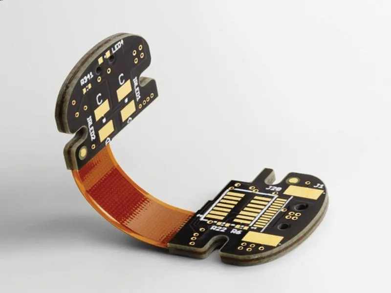
Flexible printed circuit boards (flex PCBs) are a game-changer in modern electronics. Unlike rigid boards, flex PCBs can bend, fold, and twist, making them ideal for compact devices like wearables, medical equipment, and automotive systems. Their ability to conform to unique shapes reduces space and weight while maintaining reliable electrical connections.
However, designing a flex PCB isn’t as simple as swapping out a rigid board. Factors like material selection, bend radius, and dielectric thickness directly influence how the board performs under stress and in high-speed applications. Understanding these elements ensures your design meets both mechanical and electrical requirements.
Dielectric Thickness in Flex PCBs: The Basics
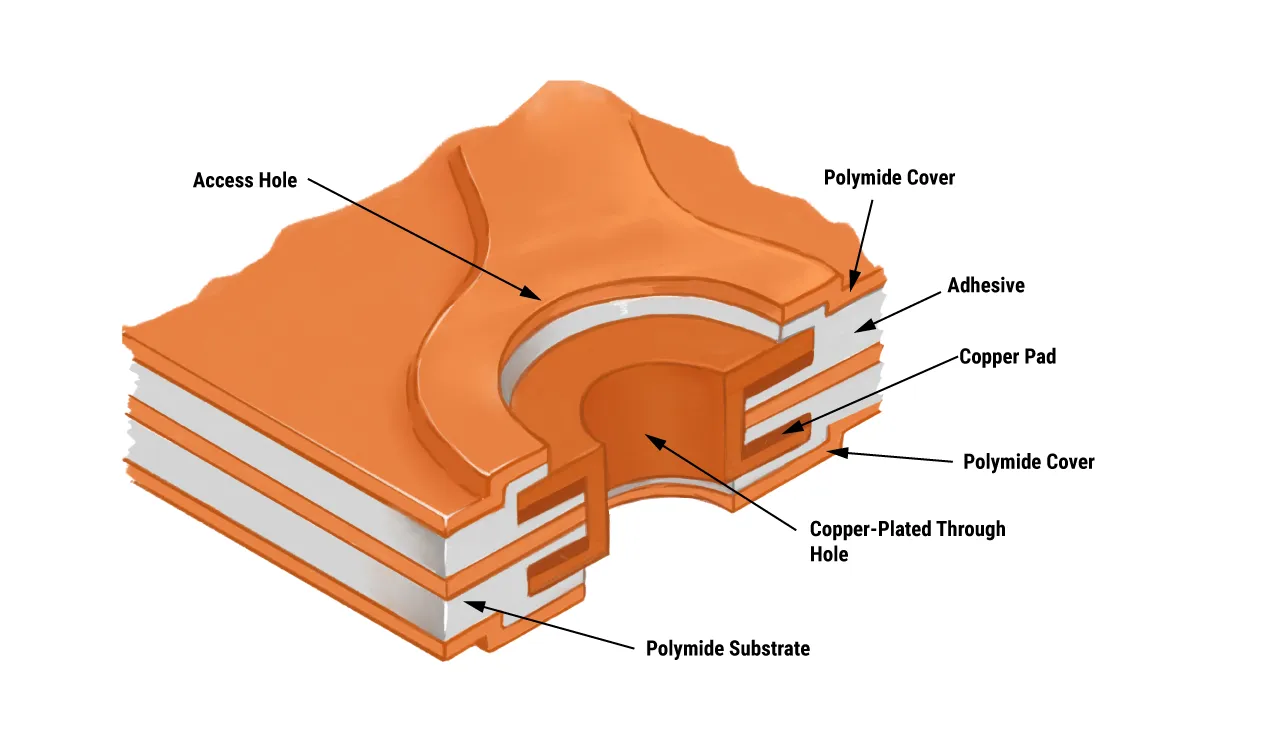
The dielectric layer in a flex PCB is the non-conductive material that separates the copper traces. Typically made from polyimide or similar flexible materials, this layer provides insulation while allowing the board to bend. Dielectric thickness refers to the measurement of this insulating layer, usually expressed in mils (thousandths of an inch) or micrometers (μm).
Common dielectric thicknesses for flex PCBs range from 0.5 mils (12.7 μm) to 2 mils (50.8 μm), though custom designs may vary. Why does this matter? The thickness of the dielectric layer directly affects two critical aspects: the board’s flexibility and its electrical performance.
How Dielectric Thickness Impacts Flexibility
Flexibility is the hallmark of a flex PCB, and dielectric thickness is a key factor in achieving the desired bend radius—the smallest radius the board can bend without damage. A thinner dielectric layer reduces the overall thickness of the PCB, making it easier to bend and fold. For instance, a flex PCB with a 0.5-mil dielectric layer can often achieve a bend radius as tight as 6 times the total board thickness, ideal for dynamic bending applications where the board flexes repeatedly.
On the other hand, a thicker dielectric layer—say, 2 mils—adds more material between layers, increasing stiffness. This can limit the bend radius to 10-12 times the board thickness, making it better suited for static flex applications where the board is bent once during installation and remains in place.
For designs requiring extreme flexibility, such as in foldable smartphones or medical implants, opting for the thinnest possible dielectric layer is often necessary. However, this must be balanced with other design needs, as we’ll explore next.
Dielectric Thickness and Electrical Performance
Beyond flexibility, dielectric thickness significantly impacts the electrical performance of a flex PCB. This is especially critical in high-speed or high-frequency applications where signal integrity is paramount.
Signal Integrity and Impedance: The dielectric thickness influences the characteristic impedance of the traces, which is crucial for maintaining signal quality. For example, in a 50-ohm impedance design, a thinner dielectric layer (e.g., 0.5 mils) requires narrower traces to achieve the target impedance, while a thicker layer (e.g., 2 mils) allows for wider traces. If not calculated correctly, this can lead to signal reflections or loss, especially at frequencies above 1 GHz.
Capacitance and Crosstalk: Thinner dielectric layers increase capacitance between adjacent traces or layers, which can lead to crosstalk—unwanted interference between signals. For high-density designs, a slightly thicker dielectric might be necessary to reduce this effect, even if it sacrifices some flexibility.
Dielectric Constant (Dk): The material’s dielectric constant, combined with its thickness, affects signal propagation speed. Polyimide, a common flex PCB material, has a Dk of around 3.5. A thinner layer with the same Dk will result in faster signal speeds but may require tighter design tolerances to avoid issues like signal skew in differential pairs.
Balancing flexibility with electrical performance often requires simulation tools and testing to fine-tune dielectric thickness for your specific application.
Flex PCB Materials and Their Role in Dielectric Thickness
The choice of material for the dielectric layer is just as important as its thickness. Most flex PCBs use polyimide due to its excellent thermal stability (up to 400°C), chemical resistance, and inherent flexibility. However, variations in polyimide formulations and other materials can influence how dielectric thickness affects performance.
For instance, some polyimide films are engineered for ultra-thin applications, allowing dielectric layers as thin as 0.3 mils while maintaining strength. Others are designed for enhanced electrical properties, with lower dielectric constants (Dk as low as 2.9) to support high-speed signals in thicker layers.
When selecting materials, consider the following:
- Thermal Requirements: If your flex PCB operates in high-temperature environments (e.g., automotive under-hood applications), ensure the material can withstand thermal expansion without cracking, regardless of thickness.
- Mechanical Stress: For dynamic bending applications, prioritize materials with high tensile strength to prevent tearing at thin dielectric thicknesses.
- Cost: Ultra-thin or specialized materials often come at a higher cost. Balance performance needs with budget constraints.
Bend Radius Considerations in Flexible PCB Design
The bend radius is a critical parameter in flexible PCB design, and dielectric thickness plays a direct role in determining what’s achievable. As a general rule, the bend radius should be at least 6-10 times the total thickness of the flex PCB for dynamic bending applications (repeated flexing) and 3-6 times for static bending (one-time installation).
For a flex PCB with a total thickness of 4 mils (including a 1-mil dielectric layer, copper, and coverlay), this translates to a minimum dynamic bend radius of 24-40 mils (0.6-1 mm). Reducing the dielectric thickness to 0.5 mils could lower the total thickness to 3 mils, allowing a tighter bend radius of 18-30 mils (0.45-0.75 mm).
However, pushing for the tightest possible bend radius by minimizing dielectric thickness isn’t always the best approach. Overly tight bends can stress the copper traces, leading to cracks or failures over time, especially in dynamic bending applications like hinges in foldable devices.
To optimize bend radius:
- Place traces perpendicular to the bend axis to minimize stress.
- Use teardrop-shaped vias to reduce stress concentration points.
- Consider adding stiffeners in non-bending areas to support connectors or components.
Dielectric Thickness in Dynamic Bending Applications
Dynamic bending applications, where the flex PCB bends repeatedly during use, demand careful consideration of dielectric thickness. Examples include robotic arms, foldable displays, and wearable sensors. In these scenarios, the board must withstand thousands or even millions of flex cycles without failure.
A thinner dielectric layer is often preferred for dynamic bending because it reduces the overall stress on the board during flexing. For instance, a flex PCB with a 0.5-mil dielectric layer can typically endure more flex cycles than one with a 2-mil layer, assuming other factors like copper thickness (commonly 0.5-1 oz, or 17-35 μm) remain constant.
However, durability isn’t just about thickness. The material’s fatigue resistance and the design of the bend area also matter. Testing under real-world conditions is essential to ensure the chosen dielectric thickness can handle the expected flex cycles without delamination or trace failure.
Practical Tips for Optimizing Dielectric Thickness in Flex PCB Design
Designing a flex PCB that balances flexibility and performance requires a strategic approach to dielectric thickness. Here are some practical tips to guide your process:
- Define Application Needs: Determine whether your design prioritizes flexibility (e.g., tight bend radius for wearables) or electrical performance (e.g., signal integrity for high-speed data). This sets the foundation for choosing dielectric thickness.
- Simulate and Test: Use PCB design software to simulate impedance and signal performance based on dielectric thickness. Follow up with physical prototypes to test bending and durability.
- Consult Material Data Sheets: Review the specifications of flex PCB materials to understand how dielectric thickness impacts Dk, tensile strength, and thermal properties.
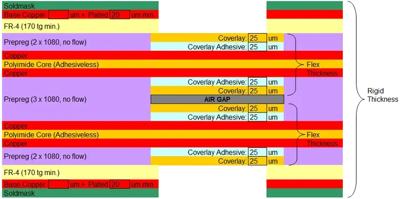
- Account for Stackup: In multilayer flex PCBs, dielectric thickness between layers affects both flexibility and interlayer capacitance. Keep inner layers thinner if flexibility is critical.
- Work with Experts: Collaborate with your manufacturing partner to ensure the chosen dielectric thickness aligns with production capabilities and cost constraints.
Conclusion: Striking the Right Balance with Dielectric Thickness
Dielectric thickness is a pivotal factor in flexible PCB design, influencing both the mechanical flexibility and electrical performance of the board. A thinner dielectric layer enhances flexibility and supports tighter bend radii, making it ideal for dynamic bending applications and compact designs. Conversely, a thicker dielectric can improve signal integrity and reduce crosstalk, which is crucial for high-speed or high-frequency circuits.
By carefully selecting flex PCB materials and optimizing dielectric thickness, you can achieve the perfect balance for your specific needs—whether it’s a wearable device, automotive system, or cutting-edge foldable tech. Understanding the interplay between dielectric thickness, bend radius, and performance ensures your design is both reliable and efficient.
Armed with these insights, you’re ready to tackle your next flex PCB project with confidence. Focus on detailed planning, material selection, and testing to bring your innovative ideas to life.


