 ALLPCB


Designing a flexible PCB layer stackup or a rigid-flex PCB involves mastering the art of balancing functionality, durability, and manufacturability. Whether you're working on a wearable device, a foldable gadget, or an industrial application, understanding flexible PCB layer stackup, rigid-flex PCB design, flex PCB materials, flexible circuit design, and dynamic bending is crucial. In this comprehensive guide, we’ll break down the essentials of layer stackup design for flex and rigid-flex circuits, offering practical tips and insights to help you create reliable and high-performing designs.
At its core, a successful flex or rigid-flex design hinges on selecting the right materials, optimizing the stackup for bending, and following best practices for manufacturing. Let’s dive into the details to help you navigate these complex designs with confidence.
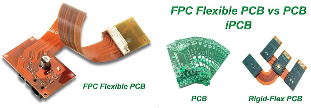
What Are Flex and Rigid-Flex PCBs?
Flex PCBs, or flexible printed circuit boards, are designed to bend and flex during use or installation. They are often used in compact or dynamic applications where traditional rigid boards can’t fit or perform. Rigid-flex PCBs combine the best of both worlds—rigid sections for structural support and flexible sections for adaptability. These hybrid boards are common in modern electronics like smartphones, medical devices, and aerospace systems.
Understanding the differences and applications of these boards is the first step in mastering flexible circuit design. Flex PCBs typically consist of thin, flexible substrates, while rigid-flex designs integrate multiple layers of both rigid and flexible materials into a single board. This combination allows for complex 3D configurations, saving space and reducing the need for connectors.
Key Considerations for Flexible PCB Layer Stackup
A flexible PCB layer stackup is the arrangement of conductive and insulating layers in a flex circuit. Unlike rigid PCBs, the stackup in a flex design must account for bending stress, material flexibility, and electrical performance. Here are the critical factors to consider:
1. Layer Count and Arrangement
The number of layers in a flex PCB typically ranges from 1 to 8, depending on the complexity of the circuit. Single-layer designs are the simplest and most cost-effective, often used for basic interconnects. Multi-layer designs, on the other hand, are necessary for high-density applications but increase manufacturing challenges due to bending stress.
When arranging layers, place critical signal traces in the inner layers to protect them from mechanical stress. For example, in a 4-layer flex stackup, the top and bottom layers might handle low-speed signals, while the inner layers carry high-speed data at speeds up to 5 Gbps, ensuring signal integrity during bending.
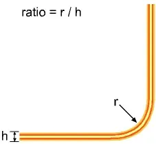
2. Bend Radius and Dynamic Bending
The bend radius is a critical parameter in dynamic bending scenarios, where the flex PCB will bend repeatedly during use. A general rule of thumb is to maintain a bend radius of at least 10 times the thickness of the flex material for dynamic applications. For a 0.1 mm thick flex layer, this means a minimum bend radius of 1 mm. Tighter bends can cause cracking or delamination of copper traces.
For static bending (one-time installation), a bend radius of 6 times the thickness may suffice. Always consult material datasheets for specific guidelines, as different substrates have varying flexibility limits.
3. Copper Weight and Trace Design
Copper weight in flex PCBs is usually lighter than in rigid boards, often ranging from 0.5 oz to 1 oz per square foot. Lighter copper reduces stress during bending but may limit current-carrying capacity. For high-current applications, consider wider traces or localized rigid sections in a rigid-flex design.
When designing traces, avoid sharp corners. Use curved or teardrop-shaped vias to minimize stress concentration. Traces should run perpendicular to the bend axis to reduce the risk of cracking. For instance, a trace width of 0.2 mm with a spacing of 0.2 mm can handle signals at 1 GHz while maintaining flexibility.
Choosing the Right Flex PCB Materials
The choice of flex PCB materials directly impacts the performance, cost, and durability of your design. Here’s a breakdown of the most common materials and their applications in flexible circuit design.
1. Base Substrates
Polyimide (PI) is the go-to material for flex PCBs due to its excellent thermal stability and flexibility. It can withstand temperatures up to 260°C, making it ideal for harsh environments. Polyester (PET) is a lower-cost alternative but offers less thermal resistance and flexibility, suitable for less demanding applications.
For high-frequency designs, consider materials with low dielectric constants (Dk) like liquid crystal polymer (LCP), which has a Dk of around 2.9, minimizing signal loss at frequencies above 10 GHz.
2. Adhesives and Coverlays
Adhesives bond the layers in a flex stackup, but they can add thickness and reduce flexibility. Adhesive-less laminates are preferred for dynamic bending applications as they reduce stress and improve reliability. Coverlays, typically made of polyimide with adhesive, protect the copper traces from environmental damage while maintaining flexibility.
3. Copper Foil Types
Rolled annealed (RA) copper is the standard for flex PCBs because it’s more ductile and can endure repeated bending without breaking. Electrodeposited (ED) copper, while cheaper, is more brittle and better suited for rigid sections in a rigid-flex design.
Rigid-Flex PCB Design: Best Practices for Layer Stackup
Rigid-flex PCB design combines the complexity of rigid and flex stackups into a single board, requiring careful planning to ensure reliability. Here are some best practices to follow:
1. Transition Zones
The transition zone between rigid and flex sections is a common failure point. To minimize stress, avoid placing vias or components near this area. Extend the flex material slightly into the rigid section (about 0.5 mm) to create a smoother transition. Additionally, stagger the layers in the transition zone to distribute stress evenly.
2. Layer Stackup Symmetry
Maintain symmetry in the layer stackup to prevent warping during manufacturing. For example, in a 6-layer rigid-flex design, pair a 2-layer flex section with a 4-layer rigid section, ensuring that the dielectric thicknesses are balanced. A typical dielectric thickness for flex layers is 0.05 mm, while rigid layers might use 0.2 mm prepreg for structural support.
3. Stiffeners for Support
In areas where additional mechanical support is needed, such as under connectors or components, add stiffeners. These are often made of polyimide or FR4 and can be bonded to the flex section without affecting its bending capability elsewhere. A stiffener thickness of 0.2 mm is common for supporting surface-mount components.
Dynamic Bending in Flex and Rigid-Flex Designs
Dynamic bending refers to the repeated flexing of a PCB during operation, such as in wearable devices or foldable electronics. Designing for dynamic bending requires extra attention to material selection, stackup design, and testing. Here’s how to ensure reliability:
1. Minimize Layer Thickness
Thinner layers reduce stress during bending. A total stackup thickness of 0.2 mm or less is ideal for dynamic applications. For instance, a 2-layer flex design with 0.05 mm polyimide per layer and 0.5 oz copper can achieve over 100,000 bend cycles without failure, based on industry-standard testing.
2. Fatigue Testing and Standards
Follow industry standards like IPC-2223 for flex PCB design to ensure durability under dynamic conditions. Conduct fatigue testing by simulating bend cycles to identify potential failure points. Some designs can endure up to 200,000 cycles with proper material selection and bend radius control.
3. Avoid Stress Concentrations
Stress concentrations occur at vias, sharp bends, or component edges. Use larger annular rings (e.g., 0.3 mm) around vias to distribute stress. Route traces away from high-stress areas and reinforce critical sections with additional coverlay material.
Common Challenges and Solutions in Flex and Rigid-Flex Design
Designing for flexible PCB layer stackup and rigid-flex PCB design comes with unique challenges. Here are some common issues and how to address them:
- Delamination: This occurs when layers separate due to thermal or mechanical stress. Use adhesive-less materials or ensure proper curing during lamination to prevent this.
- Signal Integrity Issues: Flex materials have different dielectric properties than rigid materials. Match impedance by adjusting trace widths (e.g., 0.1 mm for 50-ohm impedance) and using simulation tools for high-speed signals.
- Manufacturing Tolerances: Flex PCBs require tighter tolerances due to bending. Work closely with your manufacturer to define achievable tolerances, such as ±0.05 mm for trace spacing.
Conclusion: Mastering Flex and Rigid-Flex Layer Stackup Design
Designing a flexible PCB layer stackup or a rigid-flex PCB design is both an art and a science. By carefully selecting flex PCB materials, optimizing for dynamic bending, and following best practices in flexible circuit design, you can create reliable and innovative solutions for modern electronics. Remember to prioritize bend radius guidelines, layer symmetry, and material compatibility to ensure long-term performance.
Whether you're new to flex designs or refining an existing project, these principles will help you bend the rules—literally and figuratively—to achieve outstanding results. With the right approach, your flex and rigid-flex PCBs will meet the demands of even the most challenging applications.


