 ALLPCB


Designing a cost-effective PCB for E-Readers while ensuring high performance and scalability for mass production is a critical challenge for engineers and manufacturers. By focusing on E-Reader PCB cost optimization, low-cost PCB manufacturing, and PCB assembly cost reduction, you can achieve significant savings without sacrificing quality. In this comprehensive guide, we’ll walk you through proven strategies for optimizing your E-Reader PCB design, selecting the right vendors, and implementing design for manufacturing (DFM) for E-Reader projects. Whether you're a startup or an established company, these tips will help you streamline production and reduce expenses.
Why Cost Optimization Matters for E-Reader PCB Design
E-Readers are compact, power-efficient devices that rely on carefully designed printed circuit boards (PCBs) to deliver seamless performance. However, the competitive nature of the electronics market demands that manufacturers keep production costs low while maintaining quality. Optimizing PCB design and manufacturing processes can reduce expenses by up to 30%, according to industry studies, making it a key factor in staying competitive. In this blog, we’ll explore actionable ways to achieve E-Reader PCB cost optimization and ensure your product is ready for mass production.
Key Factors in E-Reader PCB Cost Optimization
Reducing costs starts with understanding the elements that drive PCB expenses. Let’s break down the main factors and how you can optimize each for your E-Reader project.
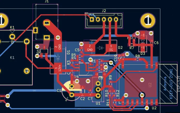
1. Simplify PCB Layout for Cost Efficiency
A complex PCB layout with intricate routing or excessive layers can significantly increase manufacturing costs. For E-Readers, which typically require low-power components and minimal high-speed signals, a simpler design often works best. Here’s how to optimize:
- Minimize Layer Count: Stick to a 2- or 4-layer PCB unless additional layers are absolutely necessary. Each additional layer can increase costs by 20-40%.
- Optimize Component Placement: Place components to reduce trace lengths and avoid crossovers, which can lower signal interference and manufacturing complexity.
- Use Standard Sizes: Design your PCB to fit standard panel sizes (e.g., 18x24 inches) to avoid material waste during production.
2. Choose Cost-Effective Materials
Material selection plays a huge role in PCB costs. E-Readers don’t usually require high-frequency materials, so you can often stick with standard options to save money.
- Use FR-4 Material: This is the most common and affordable PCB substrate, suitable for E-Reader applications with standard impedance requirements (typically around 50 ohms for digital signals).
- Avoid Exotic Finishes: Opt for standard surface finishes like HASL (Hot Air Solder Leveling) instead of more expensive options like ENIG (Electroless Nickel Immersion Gold) unless corrosion resistance is critical.
- Standard Thickness: Stick to a 1.6mm board thickness, which is widely available and cost-effective for most designs.
3. Design for Manufacturing (DFM) for E-Reader Projects
Implementing design for manufacturing (DFM) for E-Reader projects ensures that your PCB is easy to produce at scale. DFM principles help avoid costly redesigns and manufacturing delays. Consider these tips:
- Use Standard Component Sizes: Choose widely available components (e.g., 0402 or 0603 resistors) to reduce procurement costs and ensure compatibility with automated assembly machines.
- Avoid Tight Tolerances: Unless necessary, relax trace width and spacing requirements (e.g., use 6/6 mil instead of 4/4 mil) to make fabrication easier and cheaper.
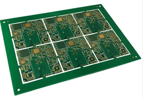
- Panelization: Design your PCB to maximize the number of boards per panel, reducing waste and lowering per-unit costs during mass production.
Strategies for Low-Cost PCB Manufacturing
Once your design is optimized, the next step is to focus on low-cost PCB manufacturing. Manufacturing costs can vary widely based on the processes, volume, and vendor capabilities. Here are some strategies to keep expenses down.
1. Leverage Economies of Scale
Mass production inherently reduces per-unit costs due to economies of scale. For E-Reader projects, aim to order in larger quantities to benefit from bulk pricing. For example, producing 1,000 units might cost $5 per board, while producing 10,000 units could drop the cost to $2 per board.
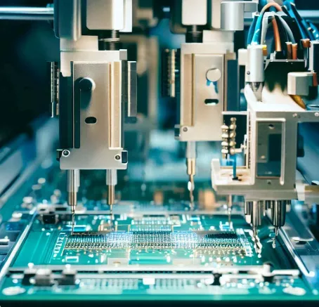
2. Optimize for Automated Assembly
Most E-Reader PCBs are assembled using automated pick-and-place machines. Designing with automation in mind can significantly reduce labor costs during PCB assembly cost reduction efforts.
- Single-Sided Assembly: Place all components on one side of the board to avoid the need for flipping during assembly, which adds time and cost.
- Standardized Footprints: Use components with common footprints to ensure compatibility with automated equipment.
3. Minimize Testing Costs
Testing is essential to ensure quality, but it can be expensive if not planned properly. For E-Readers, focus on in-circuit testing (ICT) for critical components like power management ICs and display drivers, rather than exhaustive functional testing for every board.
PCB Assembly Cost Reduction Techniques
Assembly is often one of the most expensive steps in PCB production. By focusing on PCB assembly cost reduction, you can further lower overall expenses for your E-Reader project.
1. Reduce Component Count
Fewer components mean lower material and assembly costs. For E-Readers, consider integrated solutions like System-on-Chip (SoC) designs that combine multiple functions (e.g., processor and memory) into a single chip.
2. Use Surface-Mount Technology (SMT)
SMT components are generally cheaper to assemble than through-hole components because they are compatible with automated assembly lines. For E-Reader designs, use SMT for resistors, capacitors, and ICs to save on labor costs.
3. Consolidate BOM (Bill of Materials)
A streamlined BOM reduces procurement complexity and costs. Use the same component values across your design where possible (e.g., using a single 10kΩ resistor type instead of multiple values) to simplify sourcing and assembly.
E-Reader PCB Vendor Selection: Finding the Right Partner
Choosing the right manufacturing partner is crucial for achieving cost savings and quality. When focusing on E-Reader PCB vendor selection, consider these factors to ensure a successful partnership.
1. Evaluate Manufacturing Capabilities
Ensure the vendor can handle your specific requirements, such as layer count, material type, and assembly needs. For E-Readers, look for vendors with experience in producing compact, low-power boards with high reliability.
2. Compare Pricing and Lead Times
Request quotes from multiple vendors to compare pricing for both prototyping and mass production. Also, check lead times to ensure they align with your project deadlines. Some vendors offer discounts for larger orders, which can aid in low-cost PCB manufacturing.
3. Assess Quality Control Processes
A reliable vendor should have robust quality control measures, such as Automated Optical Inspection (AOI) and X-ray testing for multilayer boards. This ensures that your E-Reader PCBs meet performance standards without costly rework.
Balancing Cost and Performance in E-Reader PCB Design
While cost optimization is critical, it’s equally important to maintain performance. E-Readers require stable power delivery, minimal signal noise, and efficient thermal management. Here’s how to strike the right balance:
- Power Management: Use efficient voltage regulators and low-power components to extend battery life, a key feature for E-Readers. Aim for a power consumption of under 1W in standby mode.
- Signal Integrity: Maintain controlled impedance for critical traces (e.g., 50 ohms for digital signals) to prevent data loss between the processor and display.
- Thermal Design: Place heat-generating components like processors away from sensitive areas, and include thermal vias if needed to dissipate heat.
Case Study: Achieving 25% Cost Reduction in E-Reader PCB Production
Consider a hypothetical scenario where a company aimed to reduce costs for their E-Reader PCB design. By implementing DFM principles, they reduced their layer count from 6 to 4, saving 15% on fabrication costs. They also switched to standard FR-4 material and optimized component placement for single-sided assembly, cutting an additional 10% from assembly expenses. Finally, by partnering with a vendor offering bulk discounts, they achieved a total cost reduction of 25% while maintaining performance standards.
Conclusion: Building Cost-Effective E-Reader PCBs for Mass Production
Designing and manufacturing cost-effective PCBs for E-Readers is a multi-step process that requires careful planning and strategic decisions. By focusing on E-Reader PCB cost optimization, adopting low-cost PCB manufacturing practices, prioritizing PCB assembly cost reduction, and making informed choices during E-Reader PCB vendor selection, you can significantly lower expenses. Implementing design for manufacturing (DFM) for E-Reader projects ensures scalability and efficiency during mass production.
Start by simplifying your design, choosing affordable materials, and partnering with a reliable vendor who understands your needs. With these strategies, you’ll be well-equipped to produce high-quality E-Reader PCBs at a fraction of the cost, helping you stay competitive in a fast-paced market.


