 ALLPCB


In the intricate world of PCB manufacturing, copper balancing stands as a critical yet often underappreciated factor in ensuring high-quality, reliable printed circuit boards. So, what is copper balancing, and why is it vital in the PCB manufacturing process? Simply put, copper balancing refers to the even distribution of copper across the layers of a PCB to prevent warping, improve manufacturability, and enhance performance. Its importance cannot be overstated—it directly impacts PCB fabrication defects, yield improvement in PCB production, and even PCB cost reduction.
In this comprehensive guide, we’ll dive deep into the role of copper balancing, exploring how it affects the PCB manufacturing process and why it’s essential for engineers and manufacturers aiming for consistent quality and efficiency. Whether you’re looking to minimize defects or optimize costs, understanding copper balancing is a game-changer.
What Is Copper Balancing in PCB Manufacturing?
Copper balancing is the practice of evenly distributing copper across the layers of a printed circuit board during the design and manufacturing stages. PCBs are made up of multiple layers of conductive copper and insulating materials, and if the copper is unevenly distributed, it can lead to mechanical stress, warping, or electrical performance issues. Achieving balance means ensuring that each layer has a similar copper density, typically within a range of 30-70% coverage, to maintain structural integrity.
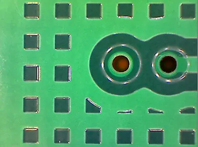
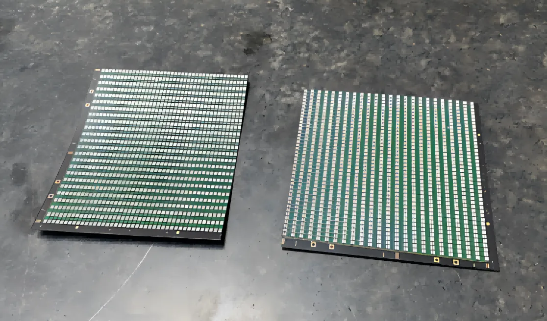
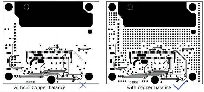
During the PCB manufacturing process, copper balancing is managed through techniques like copper thieving (adding non-functional copper patterns) and hatch patterns. These methods help fill empty spaces on the board with copper to match the density of other areas, preventing issues during etching and lamination. Without proper balancing, manufacturers risk defects that can compromise the board’s functionality and longevity.
Why Is Copper Balancing Important in PCB Manufacturing?
The importance of copper balancing in the PCB manufacturing process lies in its impact on quality, reliability, and efficiency. Let’s break down the key reasons why it matters:
1. Prevents Warping and Mechanical Stress
Uneven copper distribution creates thermal and mechanical stress during the manufacturing process. When a PCB is exposed to heat during soldering or operation, areas with higher copper density expand and contract differently than areas with less copper. This imbalance can cause the board to warp or twist, leading to misalignment of components or even cracks. Studies suggest that unbalanced copper can increase warping by up to 20% in multi-layer boards, significantly affecting reliability.
2. Improves Electrical Performance
Copper balancing also plays a role in maintaining consistent electrical performance. Uneven copper can lead to variations in impedance, especially in high-frequency designs where signal integrity is critical. For example, a poorly balanced board might exhibit impedance deviations of 10% or more, causing signal delays or data loss. Balanced copper ensures uniform current distribution, reducing the risk of hotspots and maintaining signal speeds within desired ranges, such as 3-5 ns for high-speed applications.
3. Enhances Manufacturability
From a manufacturing perspective, balanced copper distribution simplifies processes like etching and plating. During etching, areas with low copper density may over-etch, while dense areas may under-etch, leading to inconsistent trace widths. Proper balancing minimizes these risks, ensuring uniform results across the board. This directly ties into yield improvement in PCB production, as fewer boards are rejected due to manufacturing errors.
How Copper Balancing Reduces PCB Fabrication Defects
PCB fabrication defects are a major concern for manufacturers, as they lead to wasted materials, increased costs, and delayed production schedules. Copper balancing addresses several common defects, ensuring a smoother manufacturing process. Here’s how:
1. Minimizes Delamination
Delamination occurs when layers of a PCB separate due to stress or poor adhesion. Uneven copper distribution exacerbates this issue by creating stress points during thermal cycles. By balancing copper, the stress is distributed evenly, reducing the likelihood of delamination by as much as 15%, based on industry observations.
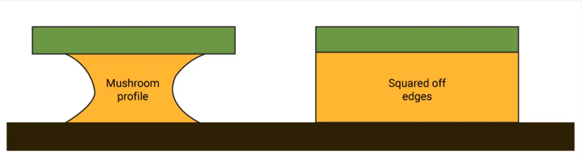
2. Reduces Etching Inconsistencies
As mentioned earlier, etching inconsistencies arise when copper density varies across the board. Over-etching in low-density areas can weaken traces, while under-etching in high-density areas can leave unwanted copper, causing shorts. Balanced copper ensures uniform etching, cutting defect rates significantly.
3. Prevents Plating Issues
During the plating process, uneven copper can lead to inconsistent deposition of materials like nickel or gold. This affects the board’s durability and conductivity. Balanced copper distribution ensures even plating, reducing defects like voids or weak solder joints that could fail under stress.
Copper Balancing for Yield Improvement in PCB Production
Yield improvement in PCB production is a top priority for manufacturers aiming to maximize output and minimize waste. Copper balancing directly contributes to higher yields by reducing the number of defective boards that need to be scrapped or reworked. Here’s how it works:
1. Fewer Manufacturing Errors
With balanced copper, the likelihood of errors during etching, lamination, and plating drops significantly. This means more boards pass quality checks on the first attempt. For instance, manufacturers have reported yield improvements of up to 10% after implementing copper balancing techniques like thieving and hatch patterns.
2. Consistent Quality Across Batches
Balanced copper ensures that each board in a batch meets the same quality standards. This consistency reduces variability, which is a common cause of low yields. When every board performs as expected, manufacturers can confidently scale production without worrying about unexpected failures.
3. Streamlined Testing and Inspection
Boards with balanced copper are less likely to fail during testing for impedance, signal integrity, or thermal performance. This speeds up the inspection process, allowing manufacturers to move boards through production faster and improve overall yield rates.
Copper Balancing and PCB Cost Reduction
Cost reduction is a critical goal in PCB manufacturing, and copper balancing offers several avenues to achieve it. While it may seem like a small detail, its impact on overall expenses is substantial. Let’s explore how it helps lower costs:
1. Reduces Material Waste
Defective boards due to unbalanced copper often need to be discarded, wasting raw materials like copper foil and laminate. By minimizing defects through proper balancing, manufacturers can reduce material waste by up to 8%, based on industry estimates, leading to significant savings over large production runs.
2. Lowers Rework Expenses
Reworking defective boards is time-consuming and costly. Balanced copper cuts down on the need for rework by ensuring boards are manufactured correctly the first time. This not only saves labor costs but also prevents delays in delivery schedules.
3. Optimizes Manufacturing Efficiency
When copper is balanced, manufacturing processes like etching and plating become more predictable and efficient. This reduces machine downtime and maintenance costs, allowing manufacturers to produce more boards in less time. Over time, these efficiency gains translate into substantial cost savings.
Best Practices for Achieving Copper Balancing in PCB Design
For engineers and designers, achieving copper balancing starts at the design stage. Here are some practical tips to ensure balanced copper distribution in your PCB layouts:
- Use Copper Thieving: Add non-functional copper shapes in empty areas of the board to match the density of other regions. This helps during etching and prevents over- or under-etching.
- Implement Hatch Patterns: In areas where solid copper isn’t needed, use hatched or grid patterns to maintain density without affecting electrical performance.
- Check Layer Symmetry: Ensure that copper distribution is mirrored across layers in multi-layer boards to avoid stress during lamination.
- Collaborate with Manufacturers: Work closely with your manufacturing partner to understand their specific requirements for copper balancing, as processes can vary.
- Use Design Software Tools: Leverage PCB design software with built-in features to analyze and balance copper density across layers.
By following these practices, designers can create layouts that are easier to manufacture and less prone to defects, ultimately improving reliability and reducing costs.
Challenges in Copper Balancing and How to Overcome Them
While copper balancing is essential, it’s not without challenges. Here are some common obstacles and solutions to address them:
1. Complex Designs with High-Density Areas
In modern PCBs, high-density interconnects (HDI) often result in uneven copper distribution. To overcome this, designers can use a combination of thieving and hatch patterns to balance density without compromising the design’s functionality.
2. Multi-Layer Board Complexity
Multi-layer boards, especially those with 6 or more layers, are prone to imbalance due to varying copper requirements on each layer. Careful planning and simulation during the design phase can help ensure symmetry and balance across all layers.
3. Cost of Additional Copper
Adding copper for balancing purposes can slightly increase material costs. However, the long-term savings from reduced defects and improved yields far outweigh the initial expense. Opt for cost-effective thieving patterns to minimize added costs.
Conclusion: Prioritizing Copper Balancing for Better PCBs
Copper balancing may be an often-overlooked aspect of the PCB manufacturing process, but its impact on quality, reliability, and cost is undeniable. By ensuring even copper distribution, manufacturers can prevent PCB fabrication defects, achieve yield improvement in PCB production, and drive significant PCB cost reduction. For engineers and designers, incorporating copper balancing techniques into the design phase is a proactive step toward creating boards that perform consistently and withstand the rigors of real-world applications.


