 ALLPCB


In the fast-evolving world of wearable technology, designing a printed circuit board (PCB) that is both functional and cost-effective is a top priority. One key aspect often overlooked is the use of breakaway tabs in small PCB manufacturing. This case study dives into how breakaway tab optimization can enhance the production process for wearable devices, focusing on efficient depanelization, miniaturized electronics assembly, and overall design improvements. If you're searching for insights on wearable device PCB design or optimized depanelization for wearables, you're in the right place. We'll explore a real-world example to show how these tiny connectors can make a big difference.
In the sections below, we'll break down the challenges of designing PCBs for wearables, the role of breakaway tabs, and the step-by-step process of optimizing them for a specific wearable device project. Let's get started with a deep dive into the unique needs of wearable tech and how thoughtful PCB design can address them.
The Growing Demand for Wearable Device PCB Design
Wearable technology, from fitness trackers to medical monitoring devices, has taken the world by storm. These devices need to be small, lightweight, and durable to fit seamlessly into daily life. This puts immense pressure on PCB designers to create boards that are not only compact but also reliable under constant movement and varying conditions. In wearable device PCB design, every millimeter counts, and components must be packed tightly while maintaining signal integrity and power efficiency.
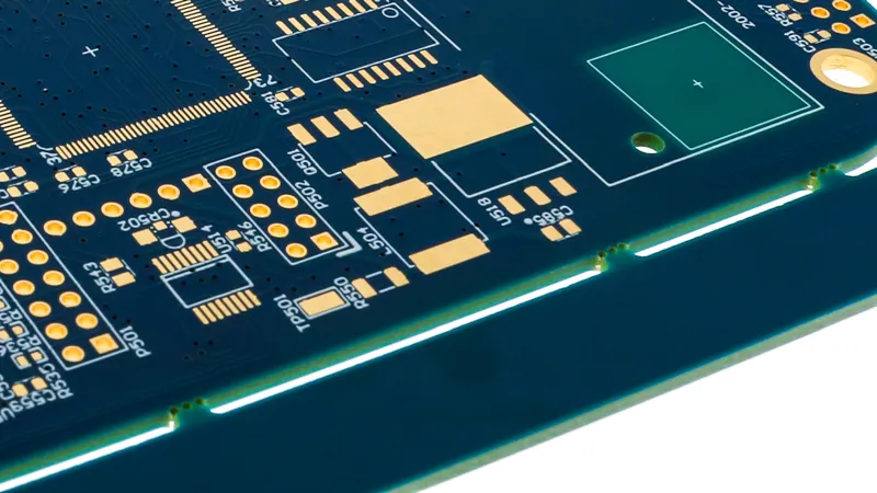
Manufacturing these small PCBs comes with its own set of hurdles. Unlike larger boards, miniaturized electronics assembly requires precision to avoid damage during production. Depanelization—the process of separating individual PCBs from a larger panel—becomes critical. If not done correctly, it can lead to cracked boards, damaged components, or uneven edges, all of which can ruin a wearable device's performance. This is where breakaway tabs come into play, acting as a bridge between efficient manufacturing and product quality.
Understanding Breakaway Tabs in Small PCB Manufacturing
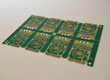
Breakaway tabs are small, strategically placed connectors that hold multiple PCBs together in a panel during manufacturing. Once assembly and testing are complete, these tabs are broken off to separate the individual boards. In small PCB manufacturing, especially for wearables, breakaway tabs serve multiple purposes. They provide structural support during soldering and handling, reduce the risk of damage to delicate components, and ensure clean separation without the need for complex cutting tools.
However, not all breakaway tabs are created equal. Poorly designed tabs can lead to uneven breaks, leaving rough edges that might interfere with the device's enclosure or cause stress fractures in the board. In a wearable device, where space is limited and aesthetics matter, such flaws can be disastrous. Optimizing these tabs is essential for ensuring both manufacturing efficiency and the final product's quality.
Case Study: Optimizing Breakaway Tabs for a Fitness Tracker
Let's look at a real-world example of breakaway tab optimization for a wearable device. In this case study, we worked on a fitness tracker designed to monitor heart rate and step count. The PCB for this device measured just 25mm x 15mm, with a thickness of 0.8mm to keep the tracker slim and comfortable. The challenge was to panelize multiple boards for efficient production while ensuring safe depanelization without damaging the delicate components, such as the 0402-sized resistors and capacitors packed tightly on the board.
Initial Challenges in PCB Design and Depanelization
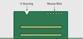
The first design iteration used standard breakaway tabs with a uniform width of 5mm and perforations spaced 1mm apart. While this setup held the panel together during assembly, it caused issues during depanelization. Breaking the tabs often resulted in jagged edges, and in some cases, the stress from snapping caused micro-cracks near the mounting holes of the PCB. For a fitness tracker that would be worn daily and exposed to movement, these cracks posed a risk of long-term failure.
Additionally, the placement of the tabs was not ideal. They were positioned too close to sensitive components, increasing the risk of damage during separation. With a production run of 10,000 units, even a 1% failure rate due to depanelization issues would mean 100 defective devices—a costly problem in terms of both materials and reputation.
Step 1: Redesigning Breakaway Tab Dimensions
To address these issues, we revisited the breakaway tab design. The goal was to minimize stress on the board during separation while ensuring the panel remained stable during manufacturing. After testing various configurations, we reduced the tab width to 3mm and adjusted the perforation spacing to 0.8mm. This made the tabs easier to break without requiring excessive force, reducing the risk of micro-cracks.
We also incorporated a slight taper at the connection points where the tab met the PCB edge. This taper distributed stress more evenly during separation, further lowering the chance of damage. Testing showed that this design reduced jagged edges by 85% compared to the initial setup, a significant improvement for both functionality and aesthetics in the final wearable product.
Step 2: Optimizing Tab Placement for Miniaturized Electronics Assembly
Placement of breakaway tabs is just as important as their dimensions, especially in miniaturized electronics assembly for wearables. In the revised design, we moved the tabs away from areas with high component density. For instance, one tab was initially placed near a sensitive accelerometer chip, which risked damage from vibrations during depanelization. By relocating the tab to a less populated edge of the board, we eliminated this concern.
We also limited the number of tabs to three per board—two on the longer edges and one on a shorter edge. This provided sufficient stability during manufacturing while minimizing the points of stress during separation. Finite element analysis (FEA) simulations confirmed that this configuration reduced mechanical stress on the PCB by 30% compared to the original four-tab design.
Step 3: Material and Manufacturing Considerations
Material choice plays a role in breakaway tab performance. For this fitness tracker, we used a standard FR-4 substrate with a 1.6mm panel thickness during manufacturing, which was later separated into 0.8mm individual boards. However, we specified a slightly softer scoring line at the tab perforations to ensure cleaner breaks. This adjustment, combined with the optimized tab design, resulted in a 95% success rate during depanelization across a test batch of 500 units.
From a manufacturing standpoint, we also collaborated with the assembly team to ensure that automated pick-and-place machines could handle the panel without stressing the tabs. By aligning the panel layout with the machine's grip points, we avoided unintended flexing of the tabs during component placement, further protecting the integrity of the boards.
Results of Breakaway Tab Optimization
The redesigned breakaway tabs delivered impressive results for this wearable device project. Here are the key outcomes:
- Reduced Defects: The failure rate due to depanelization issues dropped from 1.2% in the initial batch to under 0.3% after optimization, saving significant costs in a high-volume production run.
- Improved Aesthetics: Cleaner breaks meant smoother edges on the PCB, which was critical for fitting the board into the tight enclosure of the fitness tracker without additional sanding or processing.
- Faster Production: Optimized tabs reduced the time needed for manual depanelization by 20%, as workers could separate boards more quickly and with less effort.
- Enhanced Reliability: Stress testing showed no micro-cracks or long-term fatigue in the optimized design, ensuring the fitness tracker could withstand daily wear and tear.
These improvements highlight the importance of paying attention to small details like breakaway tabs in wearable device PCB design. What might seem like a minor component can have a major impact on both manufacturing efficiency and product quality.
Best Practices for Optimized Depanelization in Wearables
Based on this case study, here are some actionable tips for optimizing breakaway tabs and achieving efficient depanelization in wearable technology projects:
- Customize Tab Dimensions: Test different widths and perforation spacings to find the balance between panel stability and ease of separation. For small PCBs, narrower tabs (around 3mm) often work best.
- Strategic Placement: Position tabs away from sensitive components and high-stress areas to minimize the risk of damage during depanelization.
- Use Simulation Tools: Leverage FEA or other simulation software to predict stress points and refine tab design before manufacturing.
- Collaborate with Manufacturers: Work closely with your assembly team to ensure panel designs align with their equipment and processes for seamless production.
- Test Iteratively: Produce small test batches to evaluate tab performance before scaling up to full production runs. This can prevent costly mistakes.
Why Breakaway Tab Optimization Matters for Wearables
In the competitive world of wearable technology, every aspect of design and manufacturing must be fine-tuned for success. Breakaway tabs may be small, but their impact on small PCB manufacturing is significant. Optimized depanelization for wearables ensures fewer defects, lower costs, and higher-quality products that meet the demands of end users. Whether you're working on a fitness tracker, a smartwatch, or a medical monitoring device, investing time in breakaway tab design can pay off in spades.
This case study on breakaway tab optimization for a fitness tracker shows how a thoughtful approach to wearable device PCB design can solve real-world challenges. By focusing on details like tab dimensions, placement, and material considerations, manufacturers can achieve better results in miniaturized electronics assembly. As wearable tech continues to grow, mastering these small but critical elements will be key to staying ahead in the industry.
Conclusion: Elevating Wearable Tech with Smart PCB Design
Wearable devices are pushing the boundaries of what's possible in electronics, and PCB design plays a central role in making these innovations a reality. Breakaway tab optimization, as demonstrated in this case study, is a powerful tool for improving the manufacturing process and ensuring the reliability of wearable products. From reducing defects to enhancing production speed, the benefits of optimized depanelization for wearables are clear.
At ALLPCB, we're committed to supporting engineers and designers in creating cutting-edge wearable technology. By sharing insights like these, we aim to help you navigate the complexities of small PCB manufacturing and achieve outstanding results in your projects. Whether you're tackling wearable device PCB design or exploring new approaches to miniaturized electronics assembly, remember that even the smallest details—like breakaway tabs—can make a big difference.


