 ALLPCB


In today’s fast-paced electronics industry, designing printed circuit boards (PCBs) that perform reliably under high-speed conditions is a top priority. How can engineers ensure optimal signal integrity while tackling complex routing challenges? The answer lies in leveraging artificial intelligence (AI) and machine learning (ML) to revolutionize PCB design. This blog explores how AI PCB routing optimization, signal integrity AI, machine learning PCB design, and automated PCB routing tools are transforming the way PCBs are created, ensuring better performance and faster design cycles.
Whether you’re an electronics engineer or a designer looking to streamline your workflow, this post will dive deep into the benefits of AI-driven tools, practical applications, and the future of PCB design. Let’s uncover how these technologies are shaping the industry with precision and efficiency.
What Is AI PCB Routing Optimization and Why Does It Matter?
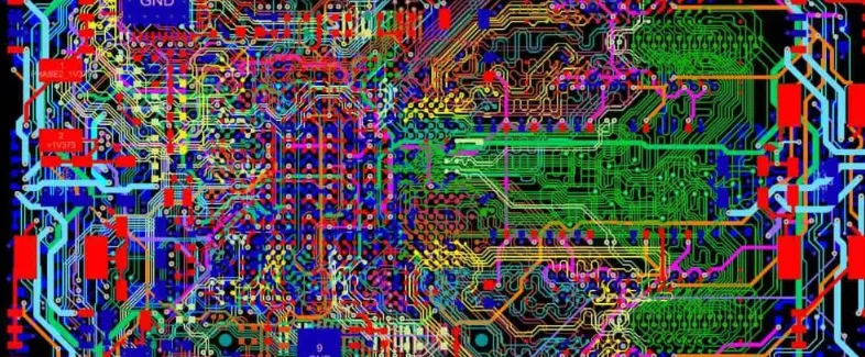
PCB routing is the process of connecting components on a board through conductive traces. Traditionally, this task has been time-consuming and prone to human error, especially in high-density designs. AI PCB routing optimization uses advanced algorithms to automate and enhance this process, reducing design time and improving accuracy. By analyzing countless design possibilities in seconds, AI identifies the most efficient paths for traces, minimizing issues like crosstalk and signal delays.
Signal integrity, on the other hand, refers to the quality of electrical signals as they travel through the PCB. Poor routing can lead to signal degradation, causing data errors or system failures. With AI, engineers can predict and mitigate these issues before they arise, ensuring reliable performance even at high frequencies, such as those exceeding 10 GHz in modern applications.
How Machine Learning Enhances PCB Design
Machine learning PCB design takes AI a step further by enabling systems to learn from vast datasets of past designs. These tools don’t just follow predefined rules; they adapt and improve over time. For instance, ML algorithms can study thousands of PCB layouts to recognize patterns that lead to optimal signal integrity or thermal performance.
One key advantage is in component placement. ML can determine the best positions for components to reduce trace lengths and avoid interference. In a real-world scenario, this might mean cutting trace lengths from 50 mm to 30 mm, reducing signal latency by up to 20%. Additionally, ML models can predict potential issues like electromagnetic interference (EMI) by analyzing historical data, allowing designers to address problems early.
Key Benefits of Machine Learning in PCB Design
- Faster Iterations: ML tools can evaluate multiple design options in minutes, compared to hours or days for manual processes.
- Error Reduction: Automated checks for signal integrity issues lower the risk of costly redesigns.
- Cost Efficiency: Optimized layouts use less board space and fewer layers, cutting manufacturing costs by as much as 15% in some cases.
Signal Integrity AI: Ensuring Reliable Performance
Signal integrity is critical in high-speed designs, where even small impedance mismatches can cause significant issues. Signal integrity AI focuses on maintaining clean, undistorted signals by optimizing trace geometry, layer stacking, and via placement. For example, AI can calculate the ideal trace width and spacing to achieve a target impedance of 50 ohms, a common standard for high-speed signals.
AI tools simulate signal behavior under various conditions, such as frequencies ranging from 1 GHz to 20 GHz. They identify potential risks like reflections or crosstalk and suggest adjustments, such as adding termination resistors or adjusting trace lengths to match signal timing. In a practical case, an AI tool might detect a 10% impedance mismatch and recommend a trace width adjustment from 0.2 mm to 0.25 mm, resolving the issue before prototyping.
Common Signal Integrity Challenges Addressed by AI
- Crosstalk: AI minimizes interference between adjacent traces by optimizing spacing and routing paths.
- Signal Delay: Tools ensure equal trace lengths for differential pairs, maintaining timing accuracy within 1 ps.
- Power Integrity: AI balances power distribution to avoid voltage drops, ensuring stable operation.
Automated PCB Routing Tools: The Future of Design
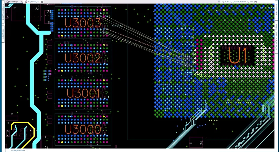
Automated PCB routing tools powered by AI are changing the game for engineers. These tools handle repetitive tasks like trace routing and via placement, freeing up time for creative problem-solving. Unlike traditional autorouters, which often produce inefficient layouts, modern AI-driven tools consider real-world constraints like manufacturing limits and signal integrity requirements.
For instance, in a multilayer PCB design, an automated tool might route 90% of traces on the first attempt while ensuring no violations of design rules, such as maintaining a minimum clearance of 0.1 mm between traces. This level of precision reduces manual adjustments and speeds up the design-to-production timeline by as much as 30%.
Features of Modern Automated Routing Tools
- Constraint-Driven Routing: Tools follow user-defined rules for trace width, spacing, and layer usage.
- Real-Time Feedback: AI provides instant alerts for potential signal integrity issues during routing.
- Integration with Simulation: Routing tools work alongside simulation software to validate designs before finalization.
Practical Applications of AI in PCB Routing and Signal Integrity
AI and ML are already making a significant impact across various industries that rely on PCB design. Here are a few examples of how these technologies are applied:
1. High-Speed Communication Devices
In devices like 5G routers and data center equipment, signal speeds often exceed 25 Gbps. AI ensures signal integrity by optimizing differential pair routing and minimizing skew to less than 5 ps, which is critical for error-free data transmission.
2. Automotive Electronics
Modern vehicles use complex PCBs for systems like advanced driver assistance (ADAS). AI tools optimize layouts to handle high-frequency signals while meeting strict size and cost constraints, reducing board area by up to 10% in some designs.
3. Consumer Electronics
For smartphones and wearables, where space is limited, AI-driven routing maximizes efficiency. It places components and routes traces to fit within tight dimensions, often achieving a 15% reduction in layer count without compromising performance.

Challenges and Limitations of AI in PCB Design
While AI offers incredible benefits, it’s not without challenges. One limitation is the need for high-quality data. Machine learning models rely on extensive datasets to deliver accurate results. If the input data is incomplete or flawed, the output may be unreliable. For example, an ML model trained on outdated designs might suggest inefficient routing paths for modern high-speed applications.
Additionally, AI tools can sometimes struggle with highly customized designs that deviate from standard patterns. In such cases, manual intervention is still necessary to fine-tune the layout. However, as AI technology evolves, these limitations are expected to diminish, with tools becoming more adaptable to unique requirements.
The Future of AI and Machine Learning in PCB Design
The future of PCB design is bright with AI and ML at the helm. As computing power increases, AI tools will handle even more complex designs, such as those for 6G technology or quantum computing, where signal integrity demands are unprecedented. We can also expect greater integration between design and manufacturing, with AI predicting production issues like thermal stress or material defects before they occur.
Moreover, cloud-based AI platforms will enable real-time collaboration among design teams worldwide, further accelerating innovation. Imagine a future where a PCB layout is optimized, simulated, and validated in under an hour, all through automated processes. This isn’t far off—industry reports suggest that AI adoption in PCB design could grow by over 25% annually through 2030.
How to Get Started with AI PCB Routing Tools
If you’re ready to integrate AI into your PCB design workflow, start by exploring software platforms that offer AI-driven features. Look for tools that support automated routing, signal integrity analysis, and machine learning capabilities. Many platforms provide tutorials and trial versions to help you understand their functionality.
Begin with smaller projects to test the tools and gradually scale up to more complex designs. Pay attention to the learning curve—while AI simplifies many tasks, understanding how to set constraints and interpret results is key to success. Over time, you’ll notice significant improvements in design speed and quality.
Conclusion: Embracing AI for Better PCB Designs
The integration of AI PCB routing optimization, signal integrity AI, machine learning PCB design, and automated PCB routing tools is transforming the electronics industry. These technologies empower engineers to create high-performing, reliable PCBs faster and more efficiently than ever before. From reducing signal delays to minimizing manufacturing costs, AI is a game-changer that no designer can afford to ignore.
At ALLPCB, we’re committed to staying at the forefront of innovation, helping you bring your ideas to life with cutting-edge solutions. By embracing AI-driven design, you can tackle the challenges of modern electronics with confidence, ensuring your products meet the highest standards of quality and performance.


