 ALLPCB


In the fast-paced world of electronics, ensuring the quality of Printed Circuit Boards (PCBs) is more critical than ever. With the rise of complex designs and high demand for precision, traditional inspection methods often fall short. This is where AI in PCB manufacturing steps in, revolutionizing quality control. By using computer vision for PCB inspection, manufacturers can achieve automated PCB defect detection with unmatched accuracy and efficiency. In this blog, we’ll dive deep into how AI-driven technologies are transforming PCB manufacturing, focusing on AI PCB quality control and the power of computer vision.
Why Quality Control Matters in PCB Manufacturing
PCBs are the backbone of almost every electronic device, from smartphones to medical equipment. A single defect, such as a misaligned component or a broken trace, can lead to device failure, costly recalls, or even safety hazards. Traditional quality control methods, like manual inspections, are time-consuming and prone to human error. Even older automated systems sometimes miss subtle defects due to limitations in detection capabilities.
With the electronics industry pushing for smaller, denser, and more intricate PCB designs, the need for precise and reliable inspection methods has skyrocketed. This is why AI PCB quality control, powered by computer vision, has become a game-changer. It offers speed, accuracy, and scalability, ensuring that defects are caught early in the production process, saving time and reducing waste.
What Is AI-Driven PCB Manufacturing?
AI-driven PCB manufacturing refers to the integration of artificial intelligence technologies into various stages of PCB production, including design, fabrication, and quality control. Specifically, in quality control, AI systems use machine learning algorithms and computer vision to analyze PCB images, identify defects, and predict potential issues before they occur.
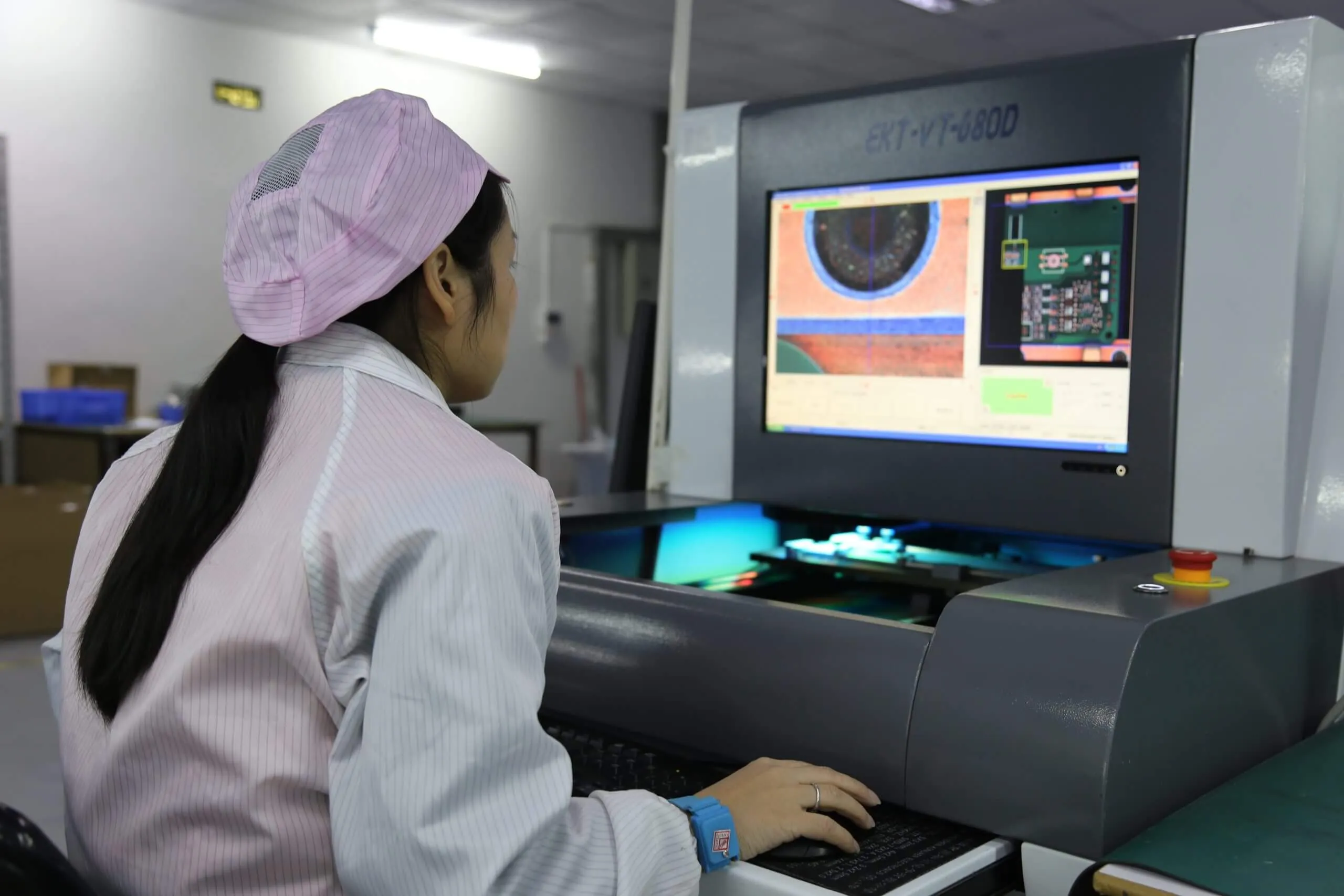
Computer vision PCB inspection involves capturing high-resolution images of PCBs during production and using AI algorithms to process these images. The system can detect anomalies such as scratches, solder joint issues, or incorrect component placements with precision that surpasses human inspectors. This automated PCB defect detection not only improves accuracy but also speeds up the inspection process, allowing manufacturers to handle higher production volumes without compromising quality.
How Computer Vision Enhances PCB Inspection
Computer vision is a branch of AI that enables machines to interpret and understand visual data, much like the human eye. In the context of PCB manufacturing, computer vision systems are trained to recognize patterns and identify deviations from the expected design. Here’s how this technology enhances PCB inspection:
1. High-Speed and Accurate Defect Detection
Unlike manual inspections that can take hours and still miss tiny flaws, computer vision systems can scan a PCB in seconds. These systems are capable of detecting defects as small as a few micrometers, ensuring that even the tiniest issues—like a hairline crack in a trace—are caught. For instance, modern systems can achieve defect detection accuracy rates above 95%, significantly reducing the risk of faulty PCBs reaching the market.
2. Real-Time Analysis for Immediate Feedback
AI-driven systems provide real-time feedback during the manufacturing process. If a defect is detected, the system can flag it instantly, allowing for immediate corrective action. This minimizes downtime and prevents the production of defective batches. Real-time analysis is especially crucial in high-volume production lines where delays can lead to significant financial losses.
3. Adaptability to Complex Designs
As PCBs become more complex with multi-layer designs and high-density interconnects, traditional inspection methods struggle to keep up. Computer vision systems, however, can be trained on diverse datasets to recognize a wide range of defects across different PCB types. Whether it’s a single-layer board or a complex multi-layer design with impedance values of 50 ohms or signal speeds exceeding 10 Gbps, AI systems adapt and deliver consistent results.
Key Benefits of AI in PCB Manufacturing for Quality Control
Integrating AI and computer vision into PCB manufacturing offers numerous advantages. Here are some of the most impactful benefits for manufacturers focusing on quality control:
1. Reduced Human Error
Human inspectors, no matter how skilled, are prone to fatigue and oversight, especially during long shifts. AI PCB quality control eliminates this issue by providing consistent, unbiased inspections. The system doesn’t get tired or distracted, ensuring every PCB is inspected with the same level of precision.
2. Cost Efficiency
While the initial investment in AI and computer vision technology may seem high, the long-term savings are substantial. By catching defects early, manufacturers avoid costly rework, scrap, and warranty claims. Additionally, automated systems reduce the need for large quality control teams, lowering labor costs.
3. Scalability for High-Volume Production
In industries where millions of PCBs are produced annually, scalability is essential. AI-driven inspection systems can handle increased workloads without sacrificing accuracy or speed. This scalability ensures that manufacturers can meet growing demand while maintaining high-quality standards.
4. Data-Driven Insights
AI systems don’t just detect defects; they also collect and analyze data over time. This data can reveal patterns, such as recurring defects in specific production stages, helping manufacturers optimize their processes. For example, if a particular soldering issue appears in 10% of boards on a specific line, the data can guide targeted improvements to eliminate the root cause.
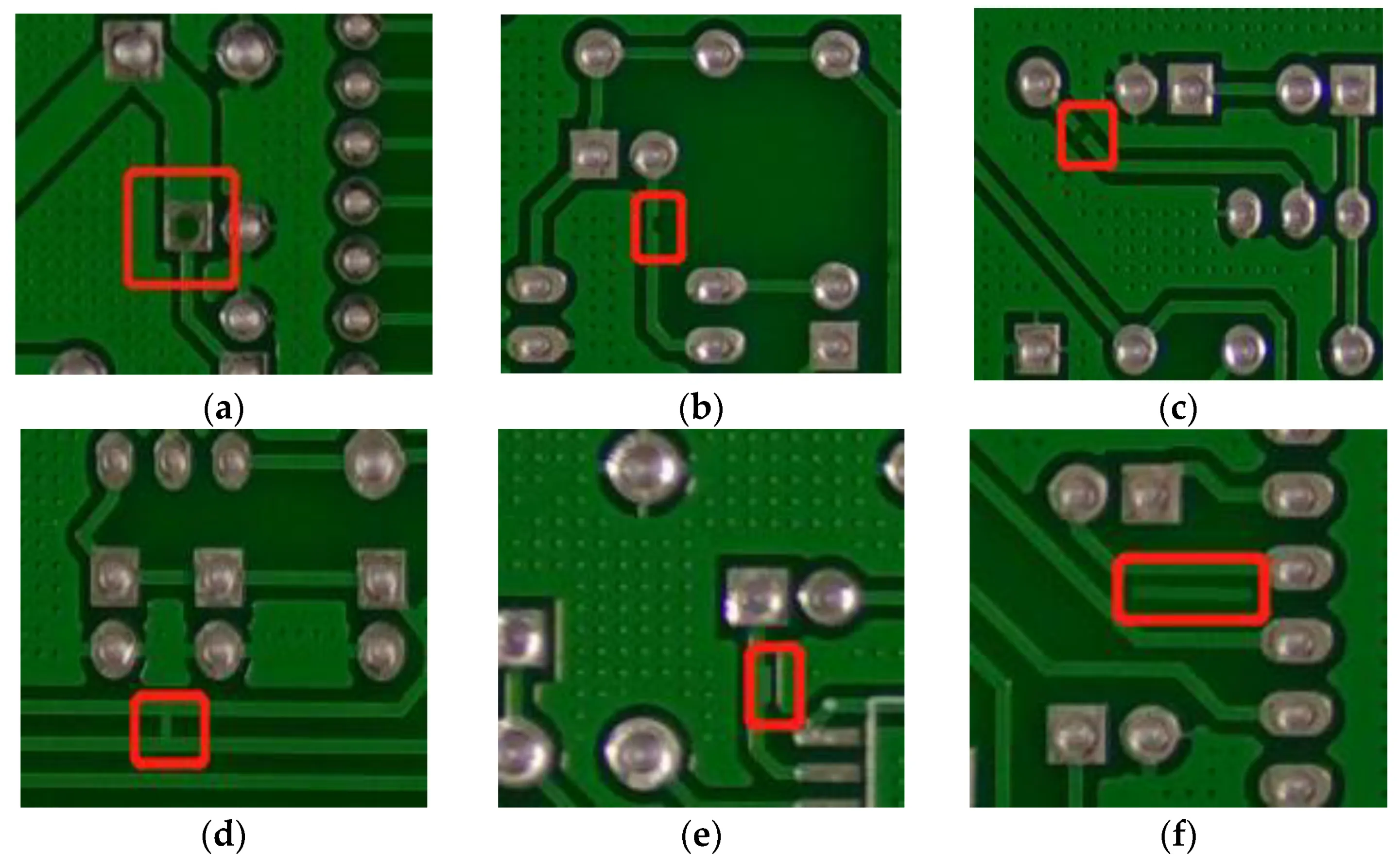
Common Defects Detected by AI and Computer Vision
AI-driven computer vision systems are trained to identify a wide range of PCB defects. Some of the most common issues include:
- Solder Joint Defects: Problems like insufficient solder, bridging, or cold joints that can affect electrical connectivity.
- Component Misplacement: Incorrectly placed or missing components that can lead to circuit failure.
- Trace Damage: Cracks or breaks in copper traces that disrupt signal flow, especially critical in high-speed designs with signal speeds of 5 Gbps or more.
- Surface Scratches: Minor scratches or contaminants on the PCB surface that could impact performance or aesthetics.
- Via Issues: Defects in vias, such as incomplete plating, which can affect multi-layer PCB functionality.
By detecting these issues early, AI systems ensure that only high-quality PCBs move forward in the production line, reducing the risk of failures in the final product.
Challenges in Implementing AI for PCB Quality Control
While the benefits of AI in PCB manufacturing are clear, there are challenges to consider during implementation. Understanding these hurdles can help manufacturers prepare and maximize the technology’s potential.
1. High Initial Costs
Setting up AI and computer vision systems requires significant investment in hardware, software, and training. Small-scale manufacturers may find the upfront costs daunting, though the long-term savings often justify the expense.
2. Need for Skilled Personnel
Operating and maintaining AI systems requires technical expertise. Manufacturers must invest in training their staff or hiring specialists to manage and update the systems, ensuring optimal performance.
3. Data Dependency
AI systems rely on large datasets to train their algorithms. Collecting and labeling high-quality data for PCB defects can be time-consuming, especially for manufacturers with limited historical data. However, once the system is trained, it continuously improves with every inspection.
Recent Advancements in AI and Computer Vision for PCB Inspection
The field of AI-driven PCB manufacturing is evolving rapidly, with new advancements enhancing the capabilities of computer vision systems. Based on recent developments, here are some cutting-edge trends shaping the future of PCB quality control:
1. Deep Learning for Nanoscale Defect Detection
Deep learning algorithms, a subset of AI, are now being used to detect defects at the nanoscale level. These systems can identify issues invisible to the human eye, ensuring even the smallest flaws are addressed during production.
2. Integration with X-Ray Inspection
For multi-layer PCBs, surface-level inspection isn’t enough. AI systems are now being paired with X-ray technologies to inspect internal layers for hidden defects like voids or misaligned vias, providing a comprehensive quality check.
3. Predictive Analytics for Process Optimization
Beyond defect detection, AI systems are using predictive analytics to foresee potential issues before they occur. By analyzing historical data, these systems can predict where defects are likely to appear, allowing manufacturers to adjust processes proactively.
How to Get Started with AI in PCB Manufacturing
For manufacturers looking to adopt AI PCB quality control, the transition doesn’t have to be overwhelming. Here are practical steps to begin integrating AI and computer vision into your production line:
- Assess Your Needs: Identify the specific quality control challenges in your production process, such as recurring defects or slow inspection times.
- Choose the Right Technology: Research AI solutions tailored for PCB inspection, focusing on systems that offer scalability and compatibility with your existing equipment.
- Start Small: Begin with a pilot project on a single production line to test the system’s effectiveness before scaling up.
- Train Your Team: Equip your staff with the skills to operate and maintain the AI system, ensuring smooth integration into daily operations.
- Monitor and Optimize: Continuously track the system’s performance and use the data insights to refine your manufacturing processes.
The Future of AI in PCB Manufacturing
The role of AI in PCB manufacturing is only set to grow. As technology advances, we can expect even smarter systems capable of self-learning and adapting to new defect types without extensive retraining. The integration of AI with other emerging technologies, like IoT and robotics, could further automate the entire PCB production process, from design to final inspection.
In the near future, AI-driven systems may also play a larger role in sustainable manufacturing. By reducing scrap rates and optimizing resource use, these systems can help manufacturers minimize waste and lower their environmental footprint. The potential for AI to transform PCB manufacturing is limitless, and early adopters stand to gain a competitive edge in the industry.
Conclusion
AI-driven PCB manufacturing, powered by computer vision, is reshaping the way quality control is conducted in the electronics industry. With automated PCB defect detection, manufacturers can achieve higher accuracy, faster inspections, and significant cost savings. Whether it’s detecting a tiny scratch on a trace or identifying a hidden defect in a multi-layer board, AI PCB quality control ensures that only the best products reach the market.
By embracing computer vision PCB inspection, manufacturers can stay ahead in a competitive landscape, delivering reliable, high-quality PCBs that meet the demands of modern electronics. The journey to AI integration may come with challenges, but the rewards—improved efficiency, reduced errors, and data-driven insights—are well worth the effort. As this technology continues to evolve, it’s clear that AI is not just a trend but a fundamental shift in how PCBs are made and inspected.


