 ALLPCB


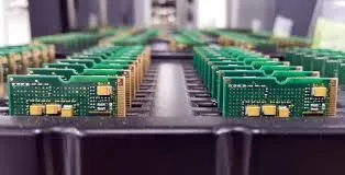
Batch assembly of printed circuit boards (PCBs) is a critical process in electronics manufacturing, but it often comes with challenges like defects that can affect performance and reliability. If you're dealing with PCB assembly defects, such as solder joint issues or component misalignment, you're not alone. This guide from ALLPCB dives deep into troubleshooting PCB errors and offers practical solutions to ensure quality control in assembly. Whether you're a seasoned engineer or a newcomer to PCB production, this post will help you identify, fix, and prevent common issues in batch-assembled PCBs.
Why Defects Happen in Batch PCB Assembly
Batch assembly involves producing multiple PCBs at once, which increases efficiency but also the risk of errors. Defects can arise from various stages, including design, soldering, component placement, and environmental factors during production. Understanding the root causes is the first step in effective troubleshooting. Common issues like poor solder joints or misaligned components often stem from inconsistent processes, inadequate equipment calibration, or material quality. By focusing on quality control in assembly, manufacturers can minimize these risks and ensure reliable outputs.
Common PCB Assembly Defects and Their Causes
Let’s explore the most frequent PCB assembly defects encountered in batch production. Identifying these issues early can save time and resources while ensuring the final product meets performance standards.
1. Solder Joint Issues
Solder joint issues are among the most common defects in PCB assembly, often leading to electrical failures or weak connections. These problems can manifest as cold solder joints, solder bridges, or insufficient solder. A cold solder joint, for instance, occurs when the solder doesn’t fully melt and bond with the component lead and pad, resulting in a dull, grainy appearance and poor conductivity. Solder bridges, on the other hand, are unintended connections between adjacent pads or traces, often caused by excessive solder or poor stencil design.
Causes:
- Inadequate soldering temperature (e.g., below 260°C for lead-free solder), leading to incomplete melting.
- Improper flux application, causing oxidation on pads or leads.
- Poor stencil alignment during solder paste application, resulting in uneven distribution.
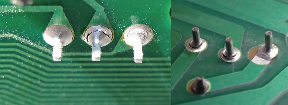
2. Component Misalignment
Component misalignment happens when parts like resistors, capacitors, or ICs are not placed correctly on the PCB during assembly. This can lead to poor connections, short circuits, or complete failure of the board. Misalignment is especially problematic in high-density designs where components are packed closely together, leaving little room for error.
Causes:
- Inaccurate pick-and-place machine calibration, with placement errors as small as 0.1 mm causing issues.
- Incorrect component footprints in the design phase, leading to mismatches during assembly.
- Vibrations or movement during reflow soldering, shifting components out of position.
3. Tombstoning
Tombstoning occurs when a small surface-mount component, like a resistor or capacitor, stands upright on one end during reflow soldering, resembling a tombstone. This defect prevents proper electrical connection and often requires rework.
Causes:
- Uneven heating during reflow, with temperature differences across the board exceeding 10°C.
- Asymmetrical pad design or solder paste application, causing one side to wet faster than the other.
- Component size or weight imbalance, particularly with smaller parts like 0402 or 0201 packages.
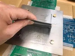
4. Insufficient or Excess Solder Paste
The amount of solder paste applied during assembly directly impacts the quality of solder joints. Too little paste can result in weak or open connections, while too much can cause bridging or short circuits.
Causes:
- Clogged or worn-out stencil apertures, reducing paste volume by up to 30% in some areas.
- Incorrect stencil thickness, typically needing to be between 0.1 mm and 0.15 mm for fine-pitch components.
- Poor storage of solder paste, leading to changes in viscosity and application consistency.
5. Open and Short Circuits
Open circuits occur when there’s a break in the connection, often due to missing solder or damaged traces. Short circuits happen when unintended connections form between traces or components, frequently caused by solder bridges or debris.
Causes:
- Damaged traces during handling, with widths as small as 0.2 mm being vulnerable to scratches.
- Contamination on the board surface, such as dust or flux residue, causing shorts.
- Inadequate spacing between traces, often less than 0.15 mm in high-density designs.
Troubleshooting PCB Errors: Step-by-Step Solutions
Once you’ve identified the defects in your batch-assembled PCBs, the next step is troubleshooting PCB errors. Below are actionable solutions tailored to the common issues discussed above, ensuring minimal downtime and optimal results.
Fixing Solder Joint Issues
For cold solder joints, reheat the joint using a soldering iron set to the appropriate temperature (around 300°C for lead-free solder) and apply fresh solder if needed. Ensure the tip is clean to avoid contamination. For solder bridges, use a desoldering braid or suction tool to remove excess solder, and inspect the stencil design to prevent recurrence. Regular calibration of reflow ovens to maintain a consistent temperature profile (e.g., peak at 245°C for 30-60 seconds) can prevent these issues in future batches.
Correcting Component Misalignment
If components are misaligned, manual rework may be necessary for small batches. Use tweezers to reposition the part and reflow the solder. For larger batches, inspect the pick-and-place machine settings and recalibrate to achieve placement accuracy within 0.05 mm. Additionally, verify the design files to ensure component footprints match the physical parts, reducing errors during assembly.
Preventing Tombstoning
To address tombstoning, adjust the reflow profile to ensure even heating, targeting a temperature ramp-up rate of 1-3°C per second. Redesign pads to be symmetrical and apply solder paste uniformly. For small components, consider using a nitrogen atmosphere during reflow to reduce oxidation and improve wetting.
Managing Solder Paste Application
Inspect stencils regularly for wear and tear, and replace them if apertures are clogged or deformed. Use a stencil thickness suited to the component pitch (e.g., 0.12 mm for 0.5 mm pitch). Store solder paste at recommended temperatures (typically 2-10°C) and mix it properly before use to maintain consistency.
Resolving Open and Short Circuits
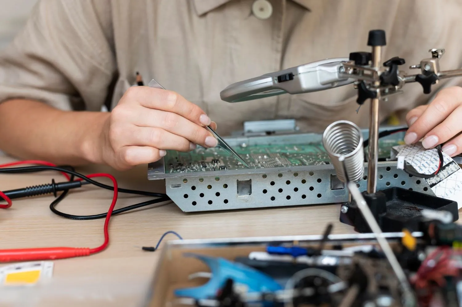
For open circuits, visually inspect the board under magnification (10x or higher) to identify breaks or missing solder, and repair with a fine-tip soldering iron. For shorts, remove excess solder or debris using a brush or compressed air, and consider adding a conformal coating post-assembly to prevent contamination. Design reviews focusing on trace spacing (minimum 0.2 mm for safety) can help avoid these issues in future designs.
Quality Control in Assembly: Best Practices to Prevent Defects
Prevention is always better than rework. Implementing robust quality control in assembly processes can significantly reduce the occurrence of defects in batch-assembled PCBs. Here are some best practices to follow:
1. Automated Optical Inspection (AOI)
Use AOI systems to detect defects like misalignment, missing components, or solder issues early in the process. These systems can scan boards at high speeds, identifying errors with an accuracy of over 95%, minimizing human error.
2. X-Ray Inspection for Hidden Defects
For complex assemblies with hidden solder joints (e.g., under BGA packages), X-ray inspection is essential. It can reveal voids or cracks in solder joints that are invisible to the naked eye, ensuring reliability in high-stakes applications.
3. Design for Manufacturability (DFM) Checks
Conduct DFM checks before production to ensure the design aligns with manufacturing capabilities. Verify pad sizes, trace widths (minimum 0.15 mm for standard processes), and component spacing to avoid assembly challenges.
4. Regular Equipment Maintenance
Calibrate and maintain assembly equipment, such as reflow ovens and pick-and-place machines, to prevent deviations. For instance, a reflow oven temperature variance of more than 5°C can lead to inconsistent soldering results.
5. Staff Training and Process Standardization
Train assembly staff on proper handling, soldering techniques, and defect identification. Standardize processes like solder paste application or component placement to ensure consistency across batches.
Advanced Tips for High-Yield PCB Assembly
For manufacturers aiming for near-perfect yields in batch production, consider advanced techniques. Use statistical process control (SPC) to monitor assembly metrics, such as defect rates per 1000 units, and identify trends for continuous improvement. Additionally, invest in high-quality materials, like solder paste with consistent particle size (Type 3 or 4 for fine-pitch applications), to reduce variability. Partnering with a reliable assembly service can also streamline these processes, ensuring expertise and precision at every step.
Conclusion
Troubleshooting PCB assembly defects like solder joint issues and component misalignment is crucial for maintaining the quality and reliability of batch-assembled PCBs. By understanding the root causes, applying targeted solutions, and prioritizing quality control in assembly, manufacturers can minimize errors and achieve consistent results. At ALLPCB, we’re committed to supporting your journey with expert guidance and top-tier assembly services. Whether you’re tackling troubleshooting PCB errors or optimizing your production line, these strategies will help you build better boards, every time.


