Are you struggling to achieve flawless solder joints in your PCB assembly process? Stencil printing is a critical step that can make or break the quality of your solder joints. In this comprehensive guide, we'll share practical solder joint tips and stencil printing techniques to help you master PCB assembly tips and perfect your soldering techniques. Whether you're a beginner or a seasoned engineer, these strategies will elevate your skills in achieving perfect solder joints.
At ALLPCB, we understand the importance of precision in electronics manufacturing. This blog post will walk you through the essentials of stencil printing, common pitfalls to avoid, and expert advice to ensure your solder joints are reliable and durable. Let's dive into the details!
Why Stencil Printing Matters for Perfect Solder Joints
Stencil printing is the foundation of modern surface-mount technology (SMT) assembly. It involves applying solder paste to the PCB through a thin metal stencil, ensuring that the right amount of paste is deposited onto the pads where components will be placed. This process directly impacts the quality of solder joints, as uneven or insufficient paste can lead to weak connections, bridging, or tombstoning.
According to industry studies, over 50% of PCB assembly defects originate from issues during the stencil printing stage. Getting this step right is crucial for achieving perfect solder joints. With the right stencil printing techniques, you can minimize defects and improve the reliability of your electronic products.

Essential Tools and Materials for Stencil Printing
Before diving into the techniques, let’s cover the basic tools and materials you’ll need for effective stencil printing:
- Stencil: Typically made of stainless steel, with laser-cut apertures matching the PCB pad layout. Stencil thickness usually ranges from 0.1mm to 0.15mm, depending on component size.
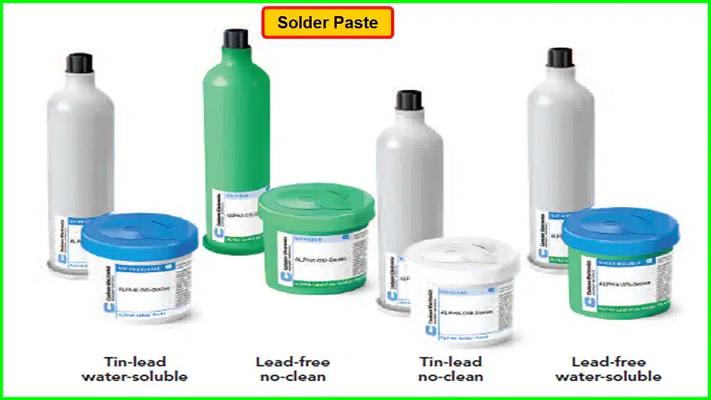
- Solder Paste: A mixture of flux and tiny solder particles. Common compositions include lead-free SAC305 (Sn96.5/Ag3.0/Cu0.5) with a melting point of around 217°C.
- Squeegee: Used to spread solder paste across the stencil. Metal squeegees are preferred for precision, often at a 45-60 degree angle.
- Printer Machine: For automated or semi-automated printing, ensuring consistent pressure and alignment.
- Inspection Tools: Microscopes or automated optical inspection (AOI) systems to check paste deposits.
Having high-quality tools is the first step in mastering PCB assembly tips for stencil printing. Ensure your equipment is clean and well-maintained to avoid contamination or inconsistent results.
Key Stencil Printing Techniques for Flawless Results
Now that you have the tools, let’s explore proven stencil printing techniques to optimize your process and achieve reliable solder joints.
1. Choose the Right Stencil Design
The stencil’s aperture design and thickness are critical for controlling solder paste volume. For fine-pitch components (e.g., 0.4mm pitch QFNs), a thinner stencil (0.1mm) with a 1:1 aperture-to-pad ratio works best. For larger components, a thicker stencil (0.15mm) with slightly reduced apertures (80-90% of pad size) prevents excess paste.
Work with your stencil manufacturer to customize the design based on your PCB layout. This tailored approach is one of the top solder joint tips to prevent issues like insufficient solder or bridging.
2. Optimize Solder Paste Selection
Not all solder pastes are created equal. Choose a paste with the correct particle size (Type 3 or Type 4 for fine-pitch applications) and flux activity level based on your reflow process. For example, Type 4 paste, with particles ranging from 20-38 microns, is ideal for components with pitches below 0.5mm.
Store solder paste at the recommended temperature (typically 2-10°C) and allow it to reach room temperature before use to avoid condensation, which can affect print quality.
3. Control Printing Parameters
Consistency in printing parameters is key to achieving perfect solder joints. Pay attention to the following settings:
- Squeegee Pressure: Typically set between 0.5-1.5 kg/cm of stencil width to ensure even paste deposition without damaging the stencil.
- Print Speed: A speed of 20-40 mm/s is ideal for most applications. Slower speeds improve paste transfer for fine-pitch components.
- Separation Speed: After printing, lift the stencil slowly (1-3 mm/s) to prevent paste from sticking to the stencil edges.
Experiment with these parameters on a test board to find the optimal settings for your specific setup.
4. Maintain Cleanliness and Alignment
Contamination is a major cause of stencil printing defects. Clean the stencil underside after every 5-10 prints using lint-free wipes and isopropyl alcohol to remove excess paste. Additionally, ensure precise alignment between the stencil and PCB using fiducial marks or automated alignment systems to avoid misprints.
Soldering Techniques to Complement Stencil Printing
Once the solder paste is applied, the next steps in the assembly process are just as important for achieving perfect solder joints. Let’s explore some key soldering techniques to ensure success during reflow.
1. Proper Component Placement
Accurate placement of components ensures the solder paste bonds correctly during reflow. Use pick-and-place machines for precision, especially for small components like 0402 resistors or fine-pitch ICs. Misalignment as small as 0.1mm can lead to defective joints or tombstoning.
2. Optimize Reflow Profile
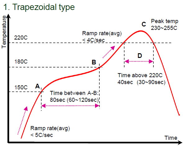
The reflow soldering process involves heating the PCB to melt the solder paste and form joints. A typical reflow profile for lead-free solder includes:
- Preheat Zone: 1-3°C/s ramp-up to 150-180°C to activate flux and prevent thermal shock.
- Soak Zone: Hold at 180-200°C for 60-120 seconds to ensure even heating.
- Reflow Zone: Peak at 235-250°C for 20-40 seconds, staying above 217°C (liquidus temperature) to melt solder.
- Cooling Zone: Cool at 2-4°C/s to solidify joints without stress.
Adjust the profile based on your board’s thermal mass and component specifications to avoid issues like cold joints or overheating.
3. Inspect Solder Joints Post-Reflow
After reflow, inspect the solder joints using visual checks, microscopes, or AOI systems. Look for:
- Shiny, concave fillets indicating good wetting.
- No cracks or voids (less than 25% of joint area as per IPC-A-610 standards).
- Proper alignment with no bridging between pads.
Early detection of defects allows for rework before the board moves to final assembly.
Common Stencil Printing and Soldering Challenges (and How to Fix Them)
Even with the best preparation, issues can arise during stencil printing and soldering. Here are some common problems and actionable PCB assembly tips to resolve them.
1. Insufficient Solder Paste Deposition
Cause: Clogged stencil apertures or low squeegee pressure.
Solution: Clean the stencil regularly and increase pressure slightly (e.g., from 0.5 to 0.8 kg/cm). If the issue persists, check if the solder paste has expired or dried out.
2. Solder Bridging
Cause: Excess paste due to oversized apertures or high printing speed.
Solution: Reduce aperture size by 10-20% for affected pads and lower print speed to 20 mm/s for better control.
3. Tombstoning
Cause: Uneven heating during reflow or imbalanced pad design.
Solution: Adjust the reflow profile for a slower ramp-up rate and ensure symmetrical pad sizes for small components like resistors and capacitors.
Advanced Tips for Mastering Solder Joints
For engineers looking to take their skills to the next level, consider these advanced solder joint tips and techniques:
- Use Step Stencils: For boards with mixed component sizes, step stencils with varying thicknesses (e.g., 0.1mm for fine-pitch areas and 0.15mm for larger components) ensure optimal paste volume across the board.
- Implement SPI (Solder Paste Inspection): Automated SPI systems measure paste height and volume after printing, detecting defects before reflow. Aim for paste height consistency within ±10% of the target.
- Monitor Environmental Conditions: Maintain a controlled environment with 40-60% humidity and 20-25°C temperature to prevent paste drying or stencil corrosion.
Why Partner with ALLPCB for Your PCB Assembly Needs
At ALLPCB, we specialize in providing high-quality PCB manufacturing and assembly services tailored to your needs. Our state-of-the-art facilities and expert team ensure precision in every step, from stencil printing to final inspection. By leveraging advanced stencil printing techniques and soldering techniques, we help you achieve flawless results for your projects.
Whether you need prototype boards or high-volume production, our commitment to quality and efficiency makes us your trusted partner in electronics manufacturing.
Conclusion: Your Path to Perfect Solder Joints
Achieving perfect solder joints starts with mastering stencil printing and refining your soldering process. By following the solder joint tips and PCB assembly tips outlined in this guide, you can minimize defects, improve reliability, and produce high-quality electronic assemblies. From selecting the right stencil design to optimizing your reflow profile, every detail matters in achieving perfect solder joints.
Put these stencil printing techniques and soldering techniques into practice on your next project, and watch your results improve. With dedication and the right approach, you’ll be well on your way to mastering PCB assembly.
 ALLPCB


