 ALLPCB


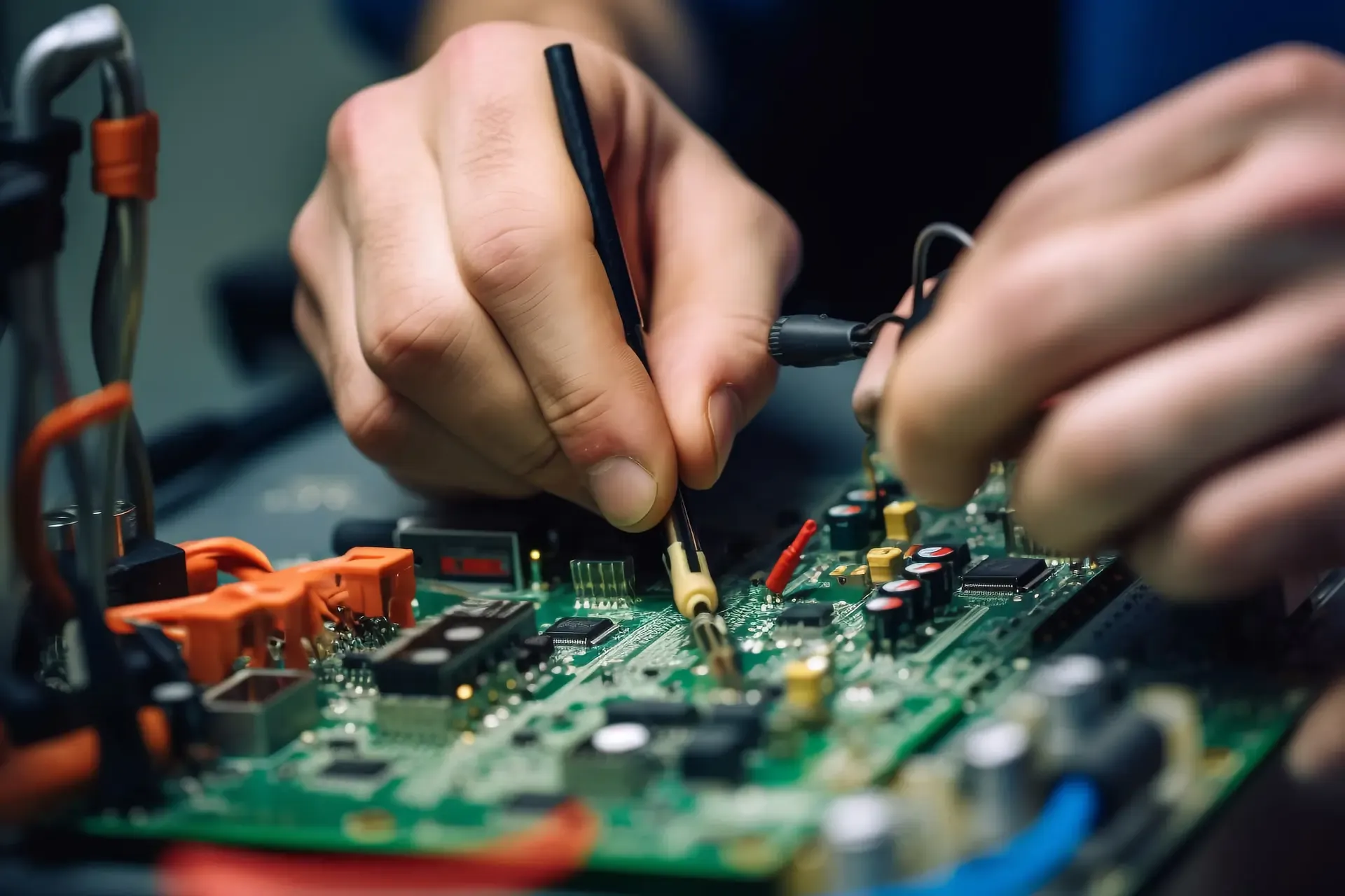
If you're looking for an efficient way to combine through-hole components with surface mount technology in PCB assembly, pin-in-paste (PIP), also known as through-hole reflow soldering, might be the perfect solution. This method offers a streamlined alternative to traditional wave soldering or selective soldering, saving time and reducing costs. In this comprehensive guide, we'll dive deep into what pin-in-paste is, how it works, its benefits, and best practices for solder paste application, helping you master this innovative technique for your projects.
What is Pin-in-Paste Soldering?
Pin-in-paste soldering is a hybrid assembly process that allows through-hole components to be soldered using the same reflow soldering process typically reserved for surface mount devices (SMDs). Instead of relying on wave soldering or hand soldering for through-hole parts, PIP involves applying solder paste to the through-hole pads or vias, inserting the component pins, and then running the board through a reflow oven. The solder paste melts and forms a strong joint around the pins during the heating process.
This technique is often seen as a wave soldering alternative because it eliminates the need for a separate soldering step, reducing production time and costs. It’s especially useful for mixed-technology boards that feature both SMD and through-hole components, ensuring a more efficient assembly workflow.
Why Choose Pin-in-Paste Over Traditional Methods?
Traditional methods like wave soldering require a separate process after SMD reflow, which can increase manufacturing time and introduce potential defects. Selective soldering, while precise, can be slow for high-volume production. Pin-in-paste, on the other hand, integrates through-hole soldering into the standard SMT reflow process, offering several advantages:
- Cost Efficiency: Reduces the need for additional equipment or labor-intensive processes.
- Time Savings: Combines SMD and through-hole soldering into a single reflow step.
- Improved Quality: Minimizes thermal stress on components by avoiding multiple heating cycles.
- Flexibility: Works well for mixed-technology PCBs with limited through-hole components.

How Does Through-Hole Reflow Soldering Work?
The pin-in-paste process might sound complex, but it follows a straightforward sequence. Let’s break it down step by step to help you understand how to implement this technique in your PCB assembly.
Step 1: PCB Design Considerations
Before you begin, the PCB design must support pin-in-paste soldering. This includes ensuring the correct hole size and pad dimensions for through-hole components. Typically, the hole diameter should be about 0.2 to 0.3 mm larger than the component pin diameter to allow for proper solder flow. The pad size around the hole should also be large enough to hold sufficient solder paste—often 1.5 to 2 times the hole diameter.
Step 2: Solder Paste Application
Solder paste application is a critical step in through-hole reflow. A stencil is used to deposit solder paste onto the pads or directly into the through-hole vias. The volume of paste must be carefully calculated to ensure a strong joint without excess solder that could cause bridging or voids. As a general rule, the paste volume should fill at least 50-75% of the hole after reflow, depending on the component and board design.
For optimal results, use a stencil thickness of 0.15 to 0.2 mm for most through-hole applications. Adjust the aperture size in the stencil to control the amount of paste deposited—larger apertures for bigger holes and pins.
Step 3: Component Placement
Once the solder paste is applied, the through-hole components are inserted into the holes. This can be done manually for low-volume production or with automated insertion machines for larger runs. Ensure the pins are fully seated in the holes to guarantee proper contact with the solder paste.
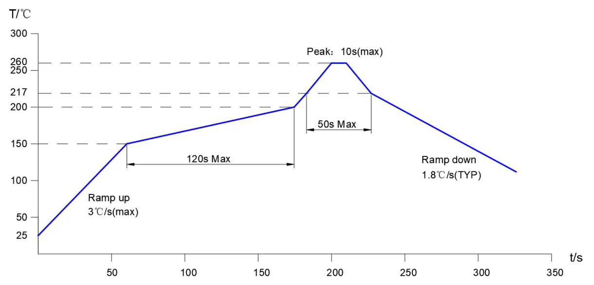
Step 4: Reflow Soldering
After component placement, the PCB goes through a reflow oven. The temperature profile must be carefully controlled to match both SMD and through-hole requirements. A typical reflow profile includes:
- Preheat Zone: Gradually heat the board to 150-180°C over 60-90 seconds to activate the flux in the solder paste.
- Soak Zone: Maintain a temperature of 180-200°C for 60-120 seconds to ensure even heating.
- Reflow Zone: Peak at 230-250°C for 20-40 seconds to melt the solder and form joints.
- Cooling Zone: Cool the board slowly to avoid thermal shock, typically over 60-90 seconds.
These values can vary based on the specific solder paste and components used, so always refer to manufacturer guidelines for the best results.
Benefits of Pin-in-Paste as a Wave Soldering Alternative
Wave soldering has been a go-to method for through-hole components for decades, but it comes with limitations, especially for modern, complex PCB designs. Pin-in-paste offers a compelling alternative by addressing many of these challenges.
Simplified Manufacturing Process
Wave soldering requires a separate step after SMT assembly, often involving additional equipment and setup. With pin-in-paste, through-hole components are soldered in the same reflow process as SMDs, streamlining production and reducing cycle time by up to 30% in some cases.
Reduced Thermal Stress
Multiple heating cycles, as seen in combined SMT reflow and wave soldering processes, can stress components and lead to failures. Pin-in-paste minimizes this risk by using a single reflow cycle, which can improve long-term reliability by reducing thermal fatigue.
Cost-Effective for Low to Medium Volumes
For small to medium production runs, setting up a wave soldering line can be expensive and time-consuming. Pin-in-paste eliminates the need for such setups, making it a more cost-effective solution for batches under 10,000 units.
Pin-in-Paste vs. Selective Soldering: Which is Better?
Selective soldering is another common method for through-hole components, especially when only a few parts need to be soldered. However, it’s worth comparing it to pin-in-paste to understand which suits your needs.
Speed and Scalability
Selective soldering uses a robotic nozzle to apply solder to specific areas, which is precise but slow for high-volume production. Pin-in-paste, integrated into the reflow process, is faster for boards with multiple through-hole components, as it solders all parts simultaneously during reflow.
Precision and Complexity
For highly dense boards where through-hole components are near sensitive SMDs, selective soldering offers better control to avoid damaging nearby parts. Pin-in-paste requires careful design to prevent solder bridging or insufficient fill, especially in tight layouts.
Cost Considerations
Selective soldering equipment can be costly to purchase and maintain, making it less ideal for smaller operations. Pin-in-paste leverages existing SMT reflow infrastructure, keeping costs lower for many manufacturers.
Best Practices for Successful Through-Hole Reflow Soldering
To achieve reliable results with pin-in-paste, follow these best practices during design and assembly. These tips are based on industry standards and real-world applications to help you avoid common pitfalls.
Optimize Hole and Pad Design
As mentioned earlier, hole size is critical. A hole that’s too small can prevent proper solder flow, while one that’s too large may not retain enough paste. Aim for a clearance of 0.2-0.3 mm between the pin and hole wall. Additionally, ensure the pad diameter is at least 1.5 times the hole size to hold adequate solder paste.
Use the Right Solder Paste
Choose a solder paste with a suitable alloy composition and particle size for through-hole applications. Type 3 or Type 4 solder paste (particle size of 25-45 μm or 20-38 μm, respectively) often works best for PIP, as it balances flow and viscosity for hole filling.
Control Solder Paste Volume
Over- or under-applying solder paste can lead to defects like voids or bridges. Use stencil design software to calculate the exact aperture size and paste volume needed. For most through-hole components, aim for 0.5-0.8 mm3 of paste per hole, adjusting based on pin and hole dimensions.
Monitor Reflow Profiles
A well-tuned reflow profile is essential to avoid issues like incomplete wetting or overheating. Use a thermal profiler to monitor the temperature across the board, ensuring it matches the solder paste manufacturer’s recommendations. Pay special attention to the peak temperature and time above liquidus to guarantee proper joint formation.
Common Challenges and How to Avoid Them
While pin-in-paste offers many benefits, it’s not without challenges. Here are some common issues and solutions to ensure high-quality results.
Solder Voids in Joints
Voids occur when air or flux gets trapped in the solder joint during reflow. To minimize this, ensure proper paste volume and use a reflow profile with a gradual preheat phase to allow outgassing. Additionally, consider using a solder paste with low-voiding properties.
Insufficient Hole Fill
If the solder doesn’t fully fill the hole, the joint may be weak. This often happens due to insufficient paste or poor pin-to-hole fit. Increase the stencil aperture size slightly or adjust the hole diameter to retain more paste during reflow.
Solder Bridging
Excess solder paste can flow between adjacent pins, causing short circuits. Prevent this by reducing paste volume and ensuring proper spacing between through-hole components in the design phase.
Applications of Pin-in-Paste Soldering
Pin-in-paste is ideal for a variety of applications, particularly in industries where mixed-technology boards are common. Some examples include:
- Automotive Electronics: For robust connectors and power components that require through-hole strength.
- Consumer Electronics: In devices with a mix of SMDs for compactness and through-hole parts for durability.
- Industrial Controls: Where reliability and cost efficiency are critical for control boards.
Conclusion: Is Pin-in-Paste Right for Your Project?
Pin-in-paste, or through-hole reflow soldering, is a powerful technique that bridges the gap between SMD and through-hole assembly. As a wave soldering alternative, it simplifies production, reduces costs, and improves reliability by minimizing thermal stress. Compared to selective soldering, it offers faster processing for many applications, though it requires careful design and process control to avoid defects.
By following the best practices outlined in this guide—optimizing PCB design, mastering solder paste application, and fine-tuning your reflow profile—you can achieve high-quality results with pin-in-paste soldering. Whether you’re working on automotive, consumer, or industrial electronics, this method can enhance your assembly process and deliver reliable, cost-effective outcomes.
Ready to implement through-hole reflow in your next project? With the right preparation and attention to detail, pin-in-paste can transform the way you approach mixed-technology PCB assembly.


