 ALLPCB


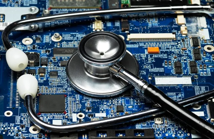
In the fast-evolving world of healthcare technology, Medical PCB Solutions are at the heart of life-saving devices like diagnostic machines, wearable monitors, and surgical tools. If you're looking for reliable ways to design, manufacture, and assemble printed circuit boards (PCBs) for medical applications, you've come to the right place. This blog dives deep into the entire process, from concept to completion, with a focus on turnkey PCB assembly and High-Density Interconnect (HDI) technology. We'll guide you through each step to ensure precision, safety, and efficiency in your medical projects.
Why Medical PCB Solutions Matter in Healthcare
Medical devices demand the highest standards of quality and reliability. A single fault in a PCB can lead to critical failures in equipment like heart monitors or imaging systems, putting patient lives at risk. That’s why specialized Medical PCB Solutions are essential. These solutions ensure that every component, connection, and layer meets strict regulatory standards, such as ISO 13485 for medical device manufacturing.
Beyond reliability, medical PCBs often need to fit into compact devices, requiring advanced technologies like HDI for tighter layouts and better performance. Whether you're developing a portable glucose meter or a complex MRI machine, the right PCB solution can make or break your project. Let’s explore how the process unfolds from design to assembly.
Designing Medical PCBs: Precision from the Start
The design phase is the foundation of any successful medical PCB project. This is where engineers define the layout, select materials, and plan for the unique challenges of medical applications. Here are the key considerations during this stage:
1. Meeting Regulatory Standards
Medical PCBs must comply with strict guidelines to ensure safety and effectiveness. Standards like ISO 13485 and IPC-6012 Class 3 (for high-reliability electronics) set the benchmark for design and manufacturing. Designers must account for biocompatibility if the PCB will be near or inside the human body, often using specific materials that prevent harmful reactions.
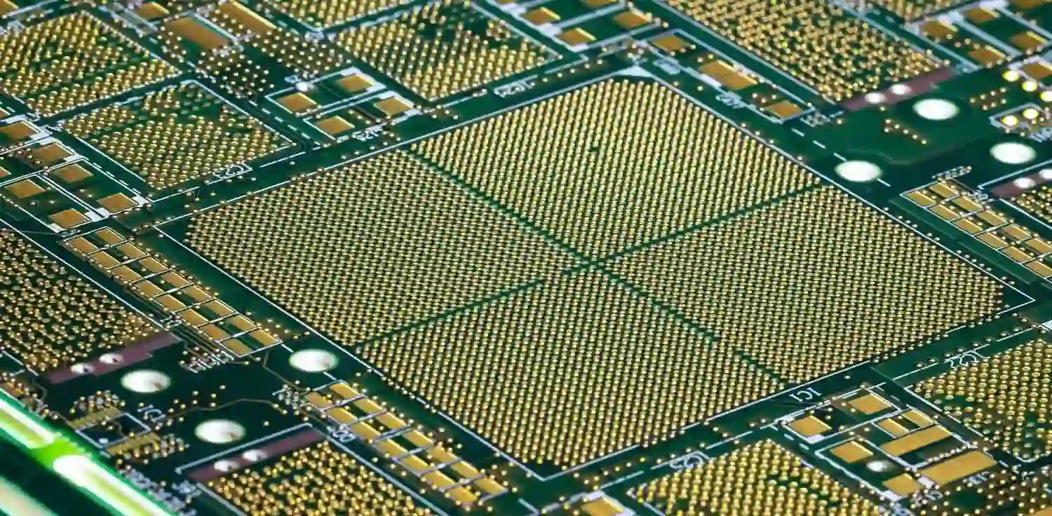
2. Incorporating HDI Technology
High-Density Interconnect (HDI) technology is a game-changer for medical PCBs. HDI allows for more components in a smaller space by using microvias and finer traces, often as small as 3 mils (0.003 inches) in width. This is critical for compact devices like hearing aids or implantable sensors. HDI also improves signal integrity, ensuring that data transmission in devices like ECG monitors remains accurate, with impedance values often controlled within ±10% tolerance for high-speed signals.
3. Thermal and Electrical Performance
Medical devices often operate in demanding conditions, so designers must prioritize thermal management and electrical reliability. For instance, a PCB in an ultrasound machine may handle high-frequency signals up to 10 MHz, requiring careful layer stacking and dielectric materials like FR-4 or polyimide to minimize signal loss.
Manufacturing Medical PCBs: Quality in Every Layer
Once the design is finalized, manufacturing begins. This stage transforms digital blueprints into physical boards, and precision is non-negotiable for medical applications. Here’s what goes into creating high-quality medical PCBs:
1. Material Selection
The choice of materials impacts both performance and safety. For medical PCBs, manufacturers often use high-grade laminates that can withstand sterilization processes or harsh environments. For example, materials with a high glass transition temperature (Tg) of 170°C or more are preferred for devices that undergo autoclaving. Additionally, lead-free soldering is common to comply with RoHS standards and avoid toxicity risks.
2. Advanced Fabrication Techniques
Manufacturing medical PCBs often involves advanced techniques to support HDI designs. Laser drilling creates microvias with diameters as small as 0.1 mm, allowing for dense component placement. Sequential lamination builds multi-layer boards—sometimes up to 20 layers or more—for complex devices like CT scanners. Each layer must align perfectly to avoid signal interference or shorts.
3. Rigorous Quality Control
Quality checks are embedded at every step. Automated Optical Inspection (AOI) systems scan for defects like misaligned traces or incomplete vias. Electrical testing ensures that impedance matches the design specs, often targeting values like 50 ohms for controlled impedance lines. For medical PCBs, failure rates must be near zero—often below 0.1%—to guarantee reliability.
Turnkey PCB Assembly: Simplifying the Process
After manufacturing, the PCB needs to be populated with components through assembly. Turnkey PCB assembly offers a complete solution, handling everything from sourcing parts to final testing. This approach is especially valuable in the medical field, where time and accuracy are critical. Let’s break down the benefits and process of turnkey assembly for medical projects.
1. What is Turnkey PCB Assembly?
Turnkey PCB assembly means entrusting the entire assembly process to a single provider. This includes procuring components, soldering them onto the board, and conducting final tests. For medical device developers, this streamlines production, reduces errors, and cuts down lead times—sometimes to as little as 48 hours for prototypes.
2. Surface Mount and Through-Hole Assembly
Medical PCBs often use a mix of Surface Mount Technology (SMT) and Through-Hole Technology (THT). SMT is ideal for tiny components in compact HDI designs, with placement accuracy down to 0.01 mm using automated pick-and-place machines. THT, on the other hand, offers durability for larger components like connectors, often found in diagnostic equipment. Both methods require precision soldering, with temperatures controlled between 260°C and 300°C to avoid damaging sensitive parts.
3. Testing and Validation
In turnkey assembly, testing is a critical final step. Functional testing verifies that the assembled PCB operates as intended, while In-Circuit Testing (ICT) checks for shorts, opens, and component values. For medical devices, additional tests like environmental stress screening may simulate operating conditions, ensuring the PCB can handle temperature swings from -20°C to 85°C without failure.
Image Placement Suggestion: Insert an image of a turnkey PCB assembly line with robotic arms placing components. ALT Text: "Turnkey PCB assembly for medical devices"
Challenges in Medical PCB Solutions and How to Overcome Them
Developing PCBs for medical use comes with unique hurdles. Understanding these challenges and their solutions can help ensure success in your projects.
1. Miniaturization Demands
As medical devices get smaller, PCBs must shrink without losing functionality. HDI technology addresses this by enabling trace widths as narrow as 2 mils and via-in-pad designs. However, this increases manufacturing complexity, so partnering with experienced providers who offer advanced fabrication capabilities is key.
2. Stringent Regulatory Compliance
Navigating regulations can be daunting. Beyond ISO standards, medical PCBs may need FDA approval in the U.S. or CE marking in Europe. Working with a provider that has a proven track record in medical projects ensures documentation and processes align with these requirements from day one.
3. Supply Chain Reliability
Component shortages can delay medical device production, which is unacceptable when lives are on the line. Turnkey PCB assembly providers often have established supply chains, sourcing components in bulk to avoid delays. Some even offer inventory management, holding stock for critical parts to ensure availability.
Benefits of Partnering with Experts for Medical PCB Solutions
Creating PCBs for medical applications is not a DIY task. Partnering with a trusted provider offers several advantages:
- End-to-End Expertise: From design to turnkey PCB assembly, experts handle every detail, reducing the risk of errors.
- Advanced Technology: Access to HDI capabilities and cutting-edge manufacturing tools ensures your PCBs meet modern demands.
- Time and Cost Efficiency: Streamlined processes cut down production time, with some providers offering prototypes in under a week, while bulk sourcing lowers component costs by up to 20%.
- Regulatory Support: Experienced teams help navigate compliance, providing documentation and testing to meet industry standards.
Future Trends in Medical PCB Solutions
The medical PCB landscape is evolving rapidly. Here are a few trends to watch:
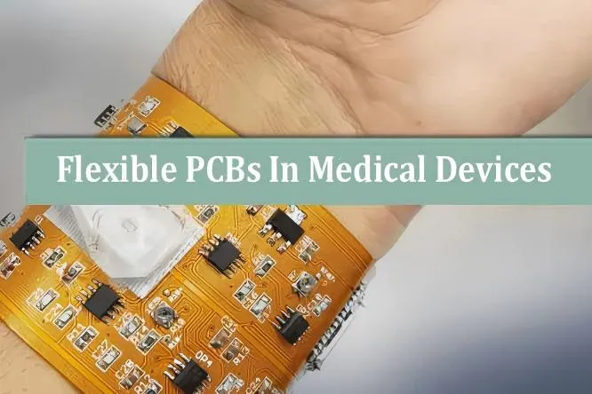
- Flexible and Wearable PCBs: Flexible materials are gaining traction for wearable health monitors, allowing PCBs to bend without breaking. These often use polyimide substrates with a thickness of just 0.1 mm.
- IoT Integration: Medical devices are increasingly connected, requiring PCBs with built-in wireless capabilities. HDI designs support the dense layouts needed for IoT chips and antennas.
- AI and Data Processing: As medical devices incorporate AI for diagnostics, PCBs must handle higher data speeds, often exceeding 5 Gbps, pushing the limits of signal integrity and layer design.
Conclusion: Your Path to Reliable Medical PCB Solutions
From intricate design using HDI technology to precision manufacturing and seamless turnkey PCB assembly, Medical PCB Solutions are the backbone of modern healthcare innovation. By understanding the process and partnering with experienced providers, you can ensure your medical devices are safe, reliable, and ready for the market. Whether you're tackling miniaturization challenges or navigating complex regulations, the right support makes all the difference in bringing life-saving technology to patients worldwide.
At ALLPCB, we’re committed to delivering top-tier solutions tailored to the unique needs of medical applications. With expertise in every stage—from design to assembly—we’re here to help you succeed in this critical field.


