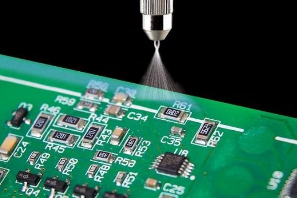
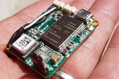
In the fast-paced world of PCB mass production, ensuring top-notch quality is non-negotiable. Automated Optical Inspection (AOI) has become a game-changer in achieving this goal by detecting defects early and maintaining consistency across thousands of boards. If you're looking to optimize quality in your production line, AOI strategies like system programming optimization, defect library creation, minimizing false positives, strategic placement in the assembly line, and data analysis for process improvement are key. This blog dives deep into these strategies, offering actionable insights to help you enhance your manufacturing process and deliver flawless printed circuit boards (PCBs) every time.
What Is Automated Optical Inspection (AOI) and Why Does It Matter?
Automated Optical Inspection, or AOI, is a technology that uses high-resolution cameras, advanced lighting, and sophisticated software to inspect PCBs for defects during manufacturing. Unlike manual inspection, which can be slow and prone to human error, AOI systems work at high speeds, catching issues like missing components, soldering defects, or incorrect placements with precision. In mass production, where thousands of boards are produced daily, AOI ensures that quality standards are met without slowing down the process.
The importance of AOI cannot be overstated. A single defective PCB can lead to costly rework, product recalls, or even failure in the field, damaging your reputation. By integrating AOI into your production line, you can reduce defect rates by up to 80%, as reported by industry studies, and save significant time and resources. Now, let’s explore specific strategies to maximize the effectiveness of AOI in your PCB manufacturing process.
1. AOI System Programming Optimization for Precision and Speed
One of the cornerstones of effective AOI implementation is programming the system for optimal performance. AOI system programming optimization involves tailoring the software algorithms to recognize specific components, board layouts, and potential defect patterns unique to your production. A poorly programmed AOI system might miss critical defects or flag too many false positives, slowing down the process.
To optimize programming, start by inputting detailed design data, such as Gerber files and bill of materials (BOM), into the AOI system. This ensures the system understands the exact specifications of your PCB, down to component sizes and placements. For instance, if your board uses 0402 resistors with a tolerance of ±5%, the AOI software should be calibrated to detect deviations beyond this range. Regular updates to the programming are also essential as production designs evolve, ensuring the system remains accurate over time.
Another tip is to adjust inspection parameters like camera resolution and lighting intensity. High-resolution settings (e.g., capturing images at 5 micrometers per pixel) can improve defect detection for fine-pitch components, though they may slow down inspection speed. Balancing precision with throughput is key—test different configurations to find the sweet spot for your production volume.
2. AOI Defect Library Creation for Accurate Detection
A well-structured AOI defect library is the backbone of reliable inspection. AOI defect library creation involves building a comprehensive database of known defects—such as tombstoning, insufficient solder, or misaligned components—that the system can reference during scans. Without a robust library, the AOI system may struggle to identify defects or misclassify normal variations as errors.
To create an effective defect library, start by collecting data from past production runs. Analyze defective boards to identify recurring issues, such as solder bridges on specific pad sizes (e.g., 0.5mm pitch connectors). Use high-quality images of these defects, taken under consistent lighting conditions, to train the AOI system. For example, if solder voids are a common issue, include images showing voids at various severity levels (e.g., 10% to 50% of pad area) to help the system differentiate between acceptable and unacceptable conditions.
Regularly update the library as new defect types emerge. If a new component type introduces unique failure modes, such as cracking in 0201 capacitors, add these to the library with clear visual examples. This continuous improvement ensures the AOI system stays relevant and accurate, even as production scales or designs change.
3. Minimizing False Positives in AOI for Efficient Production
False positives—when an AOI system flags a non-defective board as faulty—can disrupt production flow, waste time, and increase costs. Minimizing false positives in AOI is critical to maintaining efficiency while still catching real defects. Industry data suggests that false positive rates as high as 30% can occur in poorly optimized systems, leading to unnecessary manual reviews.
One way to reduce false positives is by fine-tuning inspection thresholds. For instance, if the AOI system flags slight color variations in solder paste as defects, adjust the acceptable color range (e.g., ±10% hue variation) to account for normal manufacturing differences. Similarly, set realistic tolerances for component placement—allowing a ±0.1mm offset for larger components can prevent unnecessary flags without compromising quality.
Another strategy is to use machine learning algorithms if your AOI system supports them. These algorithms can learn from past inspections, distinguishing between real defects and harmless anomalies over time. For example, after scanning 10,000 boards, the system might recognize that a specific shadow pattern on a connector isn’t a defect, reducing false calls. Combining this with regular operator feedback—where manual reviews correct AOI errors—further refines accuracy.
4. Strategic AOI Placement in the PCB Assembly Line
Where you place your AOI system in the production process can significantly impact its effectiveness. AOI placement in the PCB assembly line should be strategic, ensuring defects are caught at the earliest possible stage while minimizing disruptions to workflow. Placing AOI at the wrong point can lead to missed defects or bottlenecks in production.
A common approach is to position AOI systems at multiple stages. For instance, place one AOI unit after solder paste printing to check for issues like insufficient paste or misalignment before components are placed. Studies show that catching solder paste defects early can reduce downstream errors by up to 50%. Then, add a second AOI system after reflow soldering to inspect for issues like tombstoning or solder voids on components as small as 0.4mm pitch ICs.
For high-volume production, consider inline AOI systems that integrate seamlessly with conveyor belts, allowing continuous inspection without stopping the line. If space or budget is limited, prioritize placement after critical processes like soldering, where defects are most likely to occur. The goal is to balance thorough inspection with minimal impact on production speed—some manufacturers report achieving inspection times of under 10 seconds per board with optimal placement.
5. AOI Data Analysis for Process Improvement
Beyond detecting defects, AOI systems generate valuable data that can drive long-term improvements in your manufacturing process. AOI data analysis for process improvement involves collecting and interpreting inspection results to identify trends, root causes of defects, and areas for optimization. This proactive approach can reduce defect rates by as much as 40% over time, according to industry benchmarks.
Start by tracking defect types and frequencies. If data shows that 20% of defects are solder bridges on specific board designs, investigate upstream processes like stencil design or paste application. Adjust parameters—such as reducing paste volume by 10%—and monitor if defect rates drop. Similarly, if component misalignment spikes after a batch change, check pick-and-place machine calibration to ensure placement accuracy within ±0.05mm.
Modern AOI systems often come with built-in analytics dashboards that visualize data in real-time. Use these tools to spot patterns, such as defect spikes during certain shifts, which might indicate operator training gaps. Share this data with your team to implement targeted fixes, like adjusting reflow oven temperatures from 245°C to 240°C to reduce thermal stress on sensitive components. Over time, this data-driven approach transforms AOI from a mere inspection tool into a cornerstone of continuous improvement.
Benefits of Implementing These AOI Strategies
By adopting these AOI strategies, manufacturers can achieve significant benefits in PCB mass production. Optimized programming and defect libraries improve detection accuracy, ensuring fewer defective boards slip through. Reducing false positives saves time and labor costs associated with unnecessary rework. Strategic placement catches defects early, preventing costly downstream fixes, while data analysis drives ongoing process enhancements.
Numerically, the impact is clear. Manufacturers using well-implemented AOI systems report up to a 90% reduction in defect escapes, meaning fewer faulty boards reach customers. Production downtime can decrease by 30% due to fewer false positives and streamlined inspections. Additionally, using data to refine processes can boost overall yield by 15-20%, directly impacting profitability.
Challenges and Tips for Successful AOI Integration
While AOI offers immense benefits, integrating it into mass production isn’t without challenges. High initial costs for equipment and software can be a barrier, especially for smaller manufacturers. Complex board designs with high-density components (e.g., 0.3mm pitch BGA packages) may require advanced AOI systems with higher resolution, further increasing costs.
To overcome these challenges, start with a scalable approach. Invest in a mid-range AOI system that meets current needs but can be upgraded as production grows. Train staff thoroughly on programming and data analysis to maximize the system’s potential—poorly trained operators can negate even the best equipment. Finally, partner with a reliable PCB manufacturing service provider that offers AOI as part of their quality assurance process, reducing the burden on your in-house resources.
Conclusion: Elevate Your PCB Quality with AOI
Automated Optical Inspection is a powerful tool for maximizing quality in PCB mass production. By focusing on AOI system programming optimization, defect library creation, minimizing false positives, strategic placement in the assembly line, and data analysis for process improvement, you can ensure consistent, high-quality output while minimizing costs and delays. These strategies aren’t just about catching defects—they’re about building a smarter, more efficient production process that delivers reliable PCBs to your customers every time.
Implementing AOI effectively requires attention to detail and a commitment to continuous improvement. With the right approach, your production line can achieve unparalleled precision and reliability, setting you apart in a competitive market. Start applying these strategies today to transform your quality control and take your PCB manufacturing to the next level.
 ALLPCB


