 ALLPCB


In the fast-paced world of electronics manufacturing, precision is everything. One small mistake, like a misplaced component on a printed circuit board (PCB), can lead to costly failures or product recalls. That’s where Automated Optical Inspection (AOI) comes to the rescue. AOI systems are game-changers in detecting and preventing component misplacement, ensuring high-quality PCBs with unmatched accuracy. But how does AOI work for component placement, and why is it better than traditional methods? Let’s dive into the world of AOI component placement, PCB AOI inspection, and automatic optical inspection to understand its role in modern manufacturing.
In this blog, we’ll explore how AOI systems identify defects, why they outperform visual inspection, and how they help manufacturers save time and money. Whether you’re an engineer, a quality control specialist, or a business owner in the electronics industry, this guide will break down the essentials of AOI and its impact on PCB production.
What Is AOI and Why Does It Matter for PCB Manufacturing?
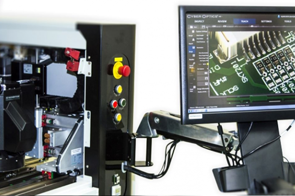
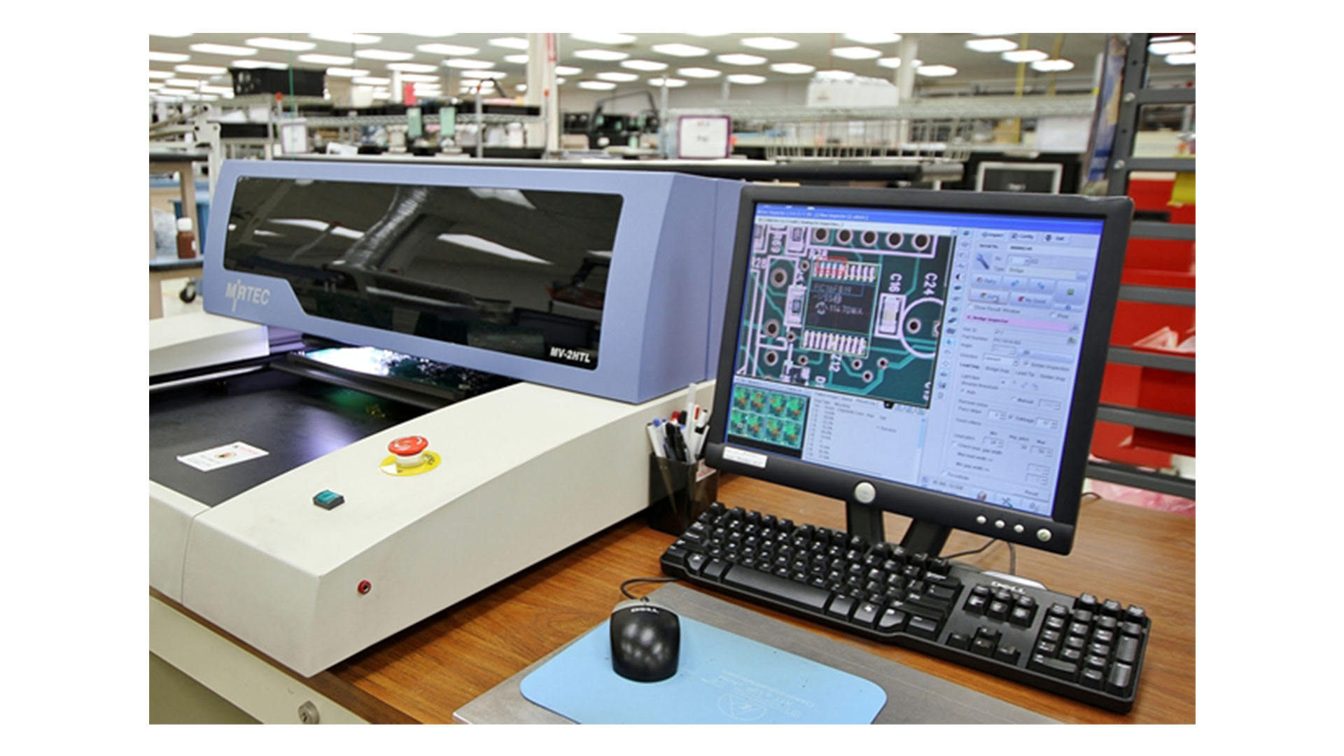
Automated Optical Inspection, or AOI, is a technology used to inspect PCBs during manufacturing. Using high-resolution cameras and advanced image processing software, AOI systems scan boards to detect defects like component misplacement, soldering issues, or missing parts. Unlike manual methods, AOI is fast, consistent, and highly accurate, making it a vital tool in today’s high-volume production lines.
In PCB manufacturing, even a tiny error can cause a circuit to fail. For instance, a misplaced resistor or capacitor can disrupt signal flow, leading to performance issues or complete device failure. AOI systems catch these problems early, often before the board moves to the next stage of assembly. By focusing on AOI component placement, manufacturers can ensure that every part is exactly where it should be, down to fractions of a millimeter.
How AOI Systems Detect Component Misplacement on PCBs
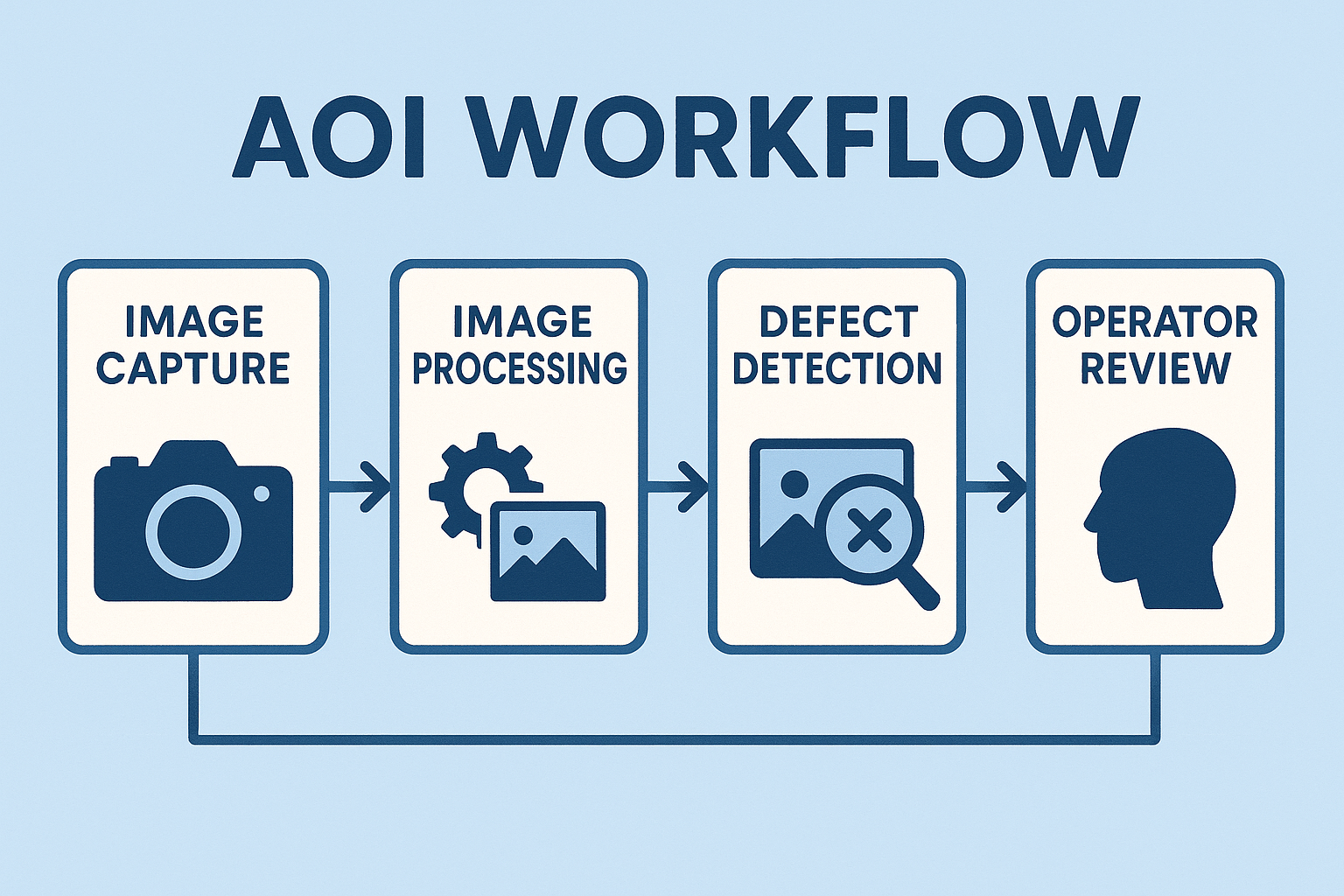
AOI systems are designed to spot even the smallest errors in PCB assembly. When it comes to component placement, these systems compare the actual board layout against a pre-programmed design file, often called a "golden board" or reference image. Here’s how the process works in simple steps:
- Image Capture: High-resolution cameras take detailed images of the PCB from multiple angles. Some advanced systems use 3D imaging to detect height variations or tilted components.
- Comparison Analysis: The AOI software compares the captured images with the design specifications. It checks for component position, orientation, and alignment with tolerances as tight as 0.01 mm.
- Defect Identification: If a component is misplaced, rotated incorrectly, or missing entirely, the system flags it as a defect. It can even detect subtle issues like tombstoning, where one end of a component lifts off the board.
- Reporting: The system generates a detailed report or visual overlay, highlighting the exact location of the error for technicians to address.
By focusing on AOI system defects, manufacturers can catch issues like a capacitor placed 0.5 mm off its pad or a diode installed in the wrong polarity. These errors might seem minor, but they can lead to short circuits or signal integrity problems, especially in high-frequency designs where impedance mismatches can occur.
Common Component Placement Defects Detected by AOI
Component misplacement is one of the most frequent issues in PCB assembly. AOI systems excel at identifying a wide range of placement-related defects, including:
- Positional Errors: Components placed outside their designated pads, often due to machine calibration issues or vibration during assembly. AOI can detect offsets as small as 0.02 mm.
- Orientation Errors: Components like diodes or ICs installed in the wrong direction, which can disrupt circuit functionality. AOI checks for correct polarity and pin alignment.
- Missing Components: Parts that fail to be placed during assembly, leaving empty pads. AOI identifies these gaps instantly.
- Tombstoning or Billboard Effects: Small components like resistors standing upright due to uneven soldering. AOI’s 3D capabilities can spot height discrepancies.
- Wrong Components: Incorrect parts placed on the board, such as a 1kΩ resistor instead of a 10kΩ one. Advanced AOI systems use pattern recognition to flag mismatches.
These defects, if undetected, can lead to costly rework or scrapped boards. With PCB AOI inspection, manufacturers can achieve defect detection rates above 95%, significantly reducing the risk of faulty products reaching customers.
AOI vs Visual Inspection: Why Automation Wins
Before AOI became widespread, visual inspection by human operators was the primary method for checking PCBs. While manual inspection still has its place for certain tasks, it falls short in several areas when compared to AOI. Let’s break down the key differences in the context of AOI vs visual inspection:
Speed and Efficiency
Visual inspection is slow and labor-intensive. A trained operator might take several minutes to inspect a single board, and complex designs with hundreds of components can take even longer. In contrast, AOI systems can scan a board in seconds, handling high-volume production lines with ease. For example, an AOI system can inspect up to 100 boards per hour, while a human might manage only 10-15 in the same time.
Accuracy and Consistency
Human inspectors are prone to fatigue and error, especially during long shifts. They might miss a misaligned component or fail to notice a subtle defect. AOI systems, on the other hand, maintain consistent accuracy, detecting defects with precision down to 0.01 mm. They don’t get tired, ensuring every board is inspected with the same level of detail.
Cost-Effectiveness
While AOI systems require an upfront investment, they save money in the long run by reducing rework and scrap rates. Visual inspection often leads to higher defect escape rates, meaning more faulty boards slip through, costing manufacturers in returns or warranty claims. AOI minimizes these losses by catching errors early.
Limitations of Visual Inspection
Manual inspection struggles with tiny components like 0201 or 01005 packages, which are common in modern compact designs. Human eyes simply can’t detect misplacements or defects at this scale without magnification tools, and even then, it’s time-consuming. AOI systems, with their high-resolution imaging, handle these challenges effortlessly.
Benefits of Using AOI for Component Placement in PCB Production
Implementing AOI systems for PCB AOI inspection offers numerous advantages, especially when it comes to ensuring proper component placement. Here are some of the key benefits:
- Improved Quality Control: AOI ensures that every component is placed correctly, reducing the risk of functional failures. This is critical for high-reliability applications like medical devices or automotive electronics, where a single error can have serious consequences.
- Faster Production Cycles: By automating inspection, AOI speeds up the manufacturing process. Boards can move from assembly to testing without delays, boosting overall throughput.
- Reduced Costs: Catching defects early prevents expensive rework or scrap. For instance, fixing a misplaced component during assembly might cost a few cents, while addressing it after shipping could cost hundreds of dollars per unit in recalls.
- Data for Process Improvement: AOI systems generate detailed reports on defect types and frequencies. Manufacturers can use this data to fine-tune assembly processes, such as adjusting pick-and-place machine settings to prevent recurring placement errors.
- Scalability: AOI systems are ideal for both small-batch and high-volume production. They can be programmed for different board designs, making them versatile for diverse product lines.
For businesses aiming to stay competitive, investing in automatic optical inspection technology is a smart move. It not only enhances product quality but also builds trust with customers by delivering reliable electronics.
Where AOI Fits in the PCB Manufacturing Process
AOI isn’t just a one-time check; it can be integrated at multiple stages of PCB production to maximize quality control. Here’s where it typically comes into play for detecting AOI system defects:
- Post-Solder Paste Inspection (SPI): Before components are placed, AOI can check the solder paste application for alignment and volume. This helps prevent placement issues caused by uneven paste.
- Pre-Reflow Inspection: After components are placed but before soldering, AOI verifies placement accuracy. This step catches misplacements early, avoiding the need to desolder components later.
- Post-Reflow Inspection: After soldering, AOI checks for both placement and soldering defects, such as bridges or insufficient solder joints. This is the most common stage for AOI use, as it covers a wide range of issues.
- Final Assembly Inspection: Before the board is encased or shipped, a final AOI scan ensures no components were dislodged during later stages.
By using AOI at multiple points, manufacturers can achieve a defect detection rate of over 98%, ensuring that only high-quality boards leave the factory.
Challenges and Limitations of AOI Systems
While AOI is a powerful tool for detecting AOI component placement issues, it’s not without challenges. Understanding these limitations helps manufacturers use the technology effectively:
- Initial Cost: AOI systems can be expensive to purchase and set up, especially for small businesses. However, the return on investment often justifies the cost through reduced defect rates.
- Programming Complexity: Setting up AOI requires creating accurate reference images or design files. Errors in programming can lead to false positives or missed defects.
- Hidden Defects: AOI primarily inspects visible surfaces. Defects under components or within multilayer boards may require additional testing methods like X-ray inspection.
- Adaptation to New Designs: Each new PCB design requires updated programming, which can slow down production during transitions.
Despite these challenges, the benefits of AOI far outweigh the drawbacks for most manufacturers, especially when paired with complementary inspection methods for comprehensive quality control.
How to Maximize AOI Effectiveness for Component Placement
To get the most out of automatic optical inspection, manufacturers should follow best practices tailored to AOI component placement:
- Regular Calibration: Ensure AOI cameras and software are calibrated regularly to maintain accuracy. Even a slight misalignment in the system can lead to incorrect defect detection.
- Optimize Lighting: Proper lighting is crucial for clear imaging. Adjust lighting conditions to avoid shadows or glare that could obscure defects.
- Update Design Files: Keep AOI reference data up to date with the latest PCB designs to prevent false alarms or missed errors.
- Train Staff: Equip technicians with the skills to interpret AOI reports and address flagged issues promptly. While AOI automates detection, human oversight is still essential for repairs.
- Integrate with Other Systems: Combine AOI with tools like Solder Paste Inspection (SPI) or In-Circuit Testing (ICT) for a holistic approach to quality control.
By fine-tuning these elements, manufacturers can achieve defect detection rates close to 99%, ensuring near-perfect PCB assembly.
Conclusion: AOI as the Future of PCB Quality Control
In the world of electronics manufacturing, precision and reliability are non-negotiable. AOI systems have emerged as indispensable tools for detecting and preventing component misplacement on PCBs, offering unmatched speed, accuracy, and cost savings compared to traditional visual inspection. From identifying tiny positional errors to ensuring correct component orientation, PCB AOI inspection helps manufacturers deliver high-quality products that meet the strictest standards.
As technology advances, AOI systems are becoming even smarter, with features like 3D imaging and artificial intelligence enhancing their capabilities. For businesses looking to stay ahead in a competitive market, adopting automatic optical inspection is not just an option—it’s a necessity. With AOI to the rescue, component misplacement and other defects don’t stand a chance, paving the way for flawless PCB production.


