 ALLPCB


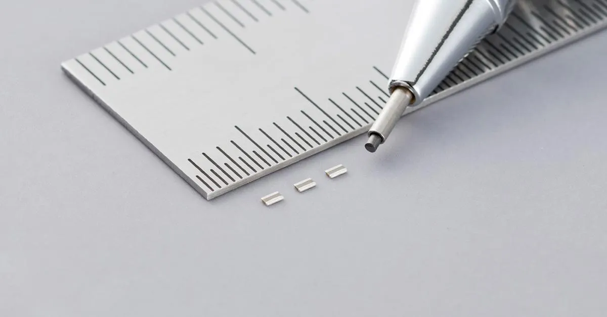
The relentless drive toward miniaturization in electronics has pushed printed circuit board (PCB) assembly to new frontiers. Among the smallest components in use today are 01005 passives - resistors and capacitors measuring just 0.4 mm x 0.2 mm. These tiny components enable compact, high-density designs critical for modern devices like smartphones, wearables, and IoT systems. However, their small size introduces significant challenges in PCB assembly, from solder paste application to placement precision and reflow profiling. In this blog, we explore the key hurdles of assembling 01005 components and share practical solutions to ensure high-yield, reliable production.
Why 01005 Components Matter
The 01005 package, named for its imperial dimensions (0.01 x 0.005 inches), represents the cutting edge of passive component miniaturization. These components are essential for high-density PCBs where space is at a premium. For instance, they can be placed between the pins of a dense ball grid array (BGA) with a pitch of 0.5 mm or less, enabling optimal signal filtering and power decoupling in compact designs like smartwatches or medical implants. Their low weight (approximately 0.04 mg) and minimal footprint make them ideal for applications requiring high functionality in small form factors, such as 5G modules or advanced RF circuits.
However, the benefits of 01005 components come with trade-offs. Their small size and light weight amplify the complexity of every assembly stage, demanding advanced equipment, precise processes, and meticulous design. Below, we dive into the primary challenges and how to address them.
Challenge 1: Precision in Solder Paste Printing
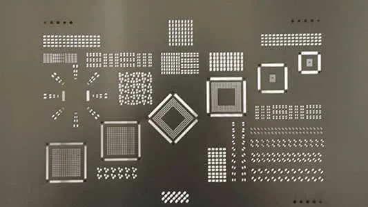
Solder paste printing is the foundation of successful 01005 assembly, but achieving consistent, accurate deposits is a formidable challenge. The pads for 01005 components are typically 200-220 µm in length and width, with a separation of 160 µm or less. This requires solder paste stencils with apertures as small as 100 µm, pushing the limits of stencil technology.
Key Issues
- Aperture Size and Area Ratio: The area ratio (the ratio of the aperture opening to the aperture wall area) is critical. For 01005 components, the area ratio often falls below 0.6, increasing the risk of incomplete paste release. According to IPC-7525 standards, low area ratios lead to inconsistent solder deposits, causing defects like tombstoning or bridging.
- Stencil Quality: Uneven stencil edges or rough aperture walls can result in uneven solder paste application. For instance, a study found that electroformed stencils achieve a process yield of 97.9%, slightly higher than the 97.5% of electropolished laser-cut stencils due to smoother aperture walls.
- Paste Type: Type 4 or Type 5 solder pastes are typically recommended for 01005 components. These finer powders (15-38 µm particle size) ensure better print definition but are prone to issues like graping if the reflow profile is not optimized.
Solutions
- Use High-Quality Stencils: Opt for electroformed or electropolished laser-cut stencils with a thickness of 75-100 µm. These provide smoother aperture walls and better paste release. Ensure a 1:1 aperture-to-pad ratio to maximize paste transfer efficiency.
- Optimize Printing Parameters: Maintain a printing speed of 8 mm/s, a print force of 5-6 kg, and a zero print gap to ensure uniform deposits. Use automated optical inspection (AOI) to verify paste volume, targeting 85-95% pad coverage.
- Select Appropriate Solder Paste: Type 5 solder paste often performs comparably to Type 4 for 01005 components, offering flexibility in high-density applications. Ensure the paste is lead-free (e.g., SAC305) to comply with RoHS standards, but be mindful of its higher melting point (217-220°C).
Challenge 2: Component Placement Accuracy
Placing 01005 components demands sub-micron precision due to their small size and tight pad spacing. Even a misalignment of 50-100 µm can lead to defects like short circuits or signal loss, compromising the board's reliability.
Key Issues
- Placement Tolerances: The 01005's footprint leaves little room for error. Misalignment can cause components to shift during reflow, leading to tombstoning (where one end lifts off the pad) or bridging (where solder connects adjacent pads).
- Equipment Limitations: Standard pick-and-place machines may struggle with the 01005's 0.04 mg weight, as their vacuum nozzles and vision systems are often optimized for larger components like 0201 or 0402.
- Component Uniformity: Mixing 01005 components with larger components, such as BGAs with a pitch greater than 25 mm, can complicate placement due to differences in thermal mass and handling requirements.
Solutions
- Advanced Placement Systems: Use high-precision pick-and-place machines with servo-motor-driven mechanisms, pneumatic nozzles, and machine-learning-enhanced vision systems. For example, a Siemens HS60 with a 1 N placement force has been shown to achieve reliable 01005 placement.
- Optimize Nozzle and Vision Settings: Select vacuum pickup nozzles designed for ultra-small components and configure vision cameras for high-resolution pattern recognition. A placement force below 3.5 N is critical to avoid cracking 01005 resistors.
- Design for Uniformity: Minimize the variety of component sizes on the PCB to streamline placement. For instance, avoid combining 01005 components with large BGAs unless thermal profiling is carefully controlled to prevent solderability issues.
Challenge 3: Reflow Soldering and Defect Prevention
The reflow soldering process for 01005 components is fraught with challenges, particularly due to the use of lead-free solder and the components' sensitivity to thermal profiles. Common defects include tombstoning, bridging, and graping (where solder joints appear concave due to incomplete flux activation).
Key Issues
- Thermal Sensitivity: Lead-free solder (e.g., SAC305) requires a peak reflow temperature of 240-245°C, which can stress 01005 components if not carefully managed. The small thermal mass of these components makes them prone to uneven heating.
- Graping: This defect occurs when flux is depleted during reflow, often due to small solder paste deposits. A study reported graping issues with 01005 components when using an RSS profile with a 1.25°C/s ramp rate and 245°C peak temperature.
- Tombstoning and Bridging: These defects arise from uneven solder paste application or inaccurate component placement. For example, a minimum spacing of 7 mils between adjacent 01005 components is necessary to prevent bridging.
Solutions
- Optimize Reflow Profiles: Use a ramp-to-spike (RTS) profile with a 1.5°C/s ramp rate, 60-second time above liquidus (TAL), and a peak temperature of 240°C to minimize graping. Avoid prolonged soak times, as they can deplete flux.
- Control Oven Atmosphere: While nitrogen atmospheres reduce oxidation, air-based reflow is viable with proper profiling. Ensure a multi-zone oven (e.g., eight zones) for precise temperature control.
- Post-Reflow Inspection: Use AOI systems calibrated to IPC-A-610 standards to detect defects like tombstoning or bridging. Microscope inspection at 40x magnification can confirm solder joint quality.
Challenge 4: Rework and Repair Difficulties
Reworking 01005 components is exceptionally challenging due to their small size and dense placement. Manual repairs are often impractical, and overheating during rework can damage adjacent components or traces.
Key Issues
- Manual Repair Limitations: The 01005's 0.4 mm x 0.2 mm footprint and 0.04 mg weight make hand soldering nearly impossible without specialized tools. Standard soldering irons lack the precision needed for such small pads.
- Thermal Damage Risk: Dense PCB layouts leave little space for rework, increasing the risk of overheating nearby components. For instance, a rework attempt on a 01005 capacitor near a BGA can compromise solder joints if the temperature exceeds 260°C.
- Limited Manufacturer Expertise: Few EMS providers have the equipment and expertise to handle 01005 rework, limiting options for high-density PCB assembly.
Solutions
- Minimize Rework Needs: Focus on first-pass yield by optimizing design and assembly processes. Use design for manufacturing and assembly (DFMA) techniques to reduce defects during initial production.
- Specialized Rework Tools: Employ precision rework stations with microscopic optics and controlled heating (e.g., hot air or laser systems) for 01005 repairs. Limit rework temperatures to 240-245°C to prevent damage.
- Partner with Experienced EMS Providers: Choose manufacturers with proven 01005 assembly capabilities, such as those certified to IPC-A-610G standards, to ensure reliable rework processes.
Challenge 5: Design and Layout Considerations
The design phase plays a critical role in overcoming 01005 assembly challenges. Poor PCB layout can exacerbate issues during printing, placement, and reflow, leading to costly failures.
Key Issues
- Pad Design and Spacing: Incorrect pad dimensions or spacing can cause defects. Optimal pad sizes for 01005 capacitors are 210 µm length, 220 µm width, and 160 µm separation; for resistors, 190 µm length, 220 µm width, and 160 µm separation. A minimum clearance of 100 µm between components is needed to avoid bridging.
- Solder Mask Definition: Choosing between solder mask defined (SMD) and non-solder mask defined (NSMD) pads affects solder joint reliability. NSMD pads are often preferred for 01005 components due to better solder flow control.
- Thermal Management: Mixing 01005 components with large thermal mass components (e.g., BGAs) can lead to uneven heating, causing solder voids or incomplete reflow.
Solutions
- Follow Manufacturer Guidelines: Adhere to component manufacturer recommendations for pad design and footprint. Ensure solder mask is defined between pads to prevent bridging.
- Use Simulation Tools: Employ PCB design software with design rule checks (DRCs) to verify pad layouts and spacing. Tools like Cadence OrCAD can help optimize 01005 layouts.
- Balance Component Selection: Design boards with uniform component sizes where possible to simplify thermal profiling and improve assembly consistency.
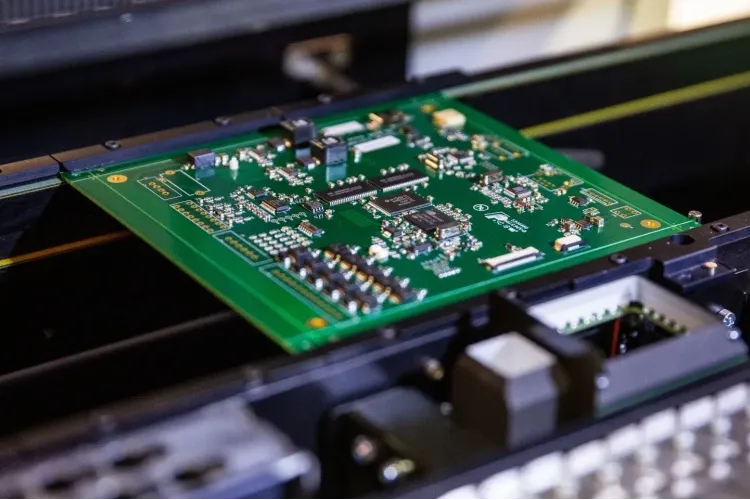
How ALLPCB Supports 01005 Assembly
At ALLPCB, we understand the complexities of assembling high-density PCBs with 01005 components. Our advanced manufacturing facilities are equipped with state-of-the-art SMT lines, including high-precision pick-and-place machines and multi-zone reflow ovens, ensuring accurate placement and reliable soldering. Our quick-turn prototyping services allow engineers to test and refine 01005 designs rapidly, while our global logistics network ensures timely delivery of components and assembled boards. By partnering with ALLPCB, you gain access to our expertise in DFMA and IPC-compliant processes, helping you overcome the challenges of 01005 assembly and bring your innovative designs to market efficiently.
Conclusion
Assembling 01005 components is a high-stakes endeavor that demands precision, advanced equipment, and careful design. From solder paste printing to reflow profiling and rework, each stage presents unique challenges that can impact yield and reliability. By adopting high-quality stencils, optimizing placement and reflow processes, and adhering to robust design practices, manufacturers can achieve successful 01005 assembly. As electronics continue to shrink, mastering these challenges will be critical for engineers pushing the boundaries of innovation. With the right strategies and partners, the potential of 01005 components can be fully realized, enabling smaller, smarter, and more powerful devices.


