ALLPCB


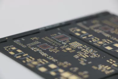
In the fast-evolving world of electronics, high-density PCBs (Printed Circuit Boards) are at the heart of cutting-edge devices, from smartphones to medical equipment. Designing these intricate boards requires precision and the right materials to ensure performance and reliability. One critical element in this process is the solder mask, a protective layer that safeguards the copper traces on a PCB. While solder masks come in various finishes, matte solder mask stands out for its unique benefits, especially in high-density PCB design. So, what are the matte solder mask benefits? Simply put, matte solder mask offers improved inspection, better prevention of solder bridging, and enhanced suitability for fine pitch components, making it a top choice for complex PCB layouts.
In this comprehensive guide, we’ll dive deep into the advantages of matte solder mask for high-density PCBs. From its role in solder bridging prevention to its impact on inspection processes, we’ll explore why this finish is gaining popularity among engineers and designers. Whether you’re working on fine pitch components or tackling intricate designs, understanding these benefits can elevate your PCB projects.
What Is a Solder Mask, and Why Does Finish Matter?
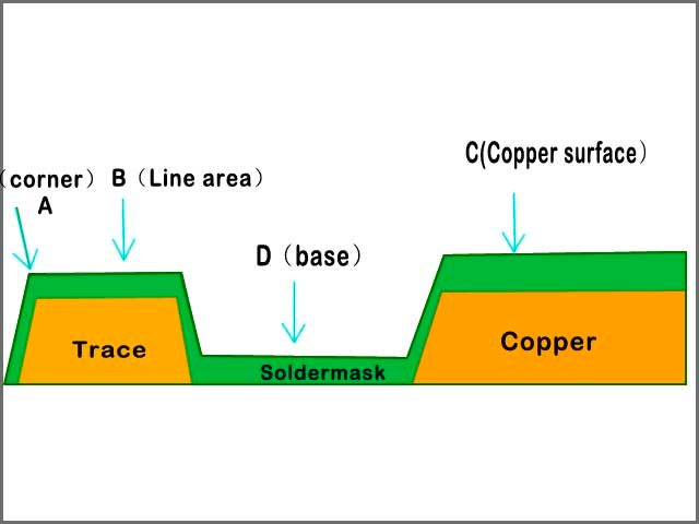
A solder mask is a thin layer of polymer applied to the copper traces of a PCB to protect them from oxidation and prevent unintended electrical connections during soldering. It acts as a barrier, ensuring that solder only adheres to the designated pads and not to the surrounding areas. Solder masks come in various colors and finishes, with glossy and matte being the most common finishes.
The finish of a solder mask isn’t just about aesthetics; it plays a significant role in functionality and manufacturability. Glossy finishes reflect light, which can sometimes interfere with inspection processes, while matte finishes diffuse light, offering practical advantages in specific scenarios. For high-density PCB design, where precision and reliability are paramount, the choice of finish can make a big difference. Let’s explore why matte solder mask is often the preferred option.
Key Benefits of Matte Solder Mask for High-Density PCBs
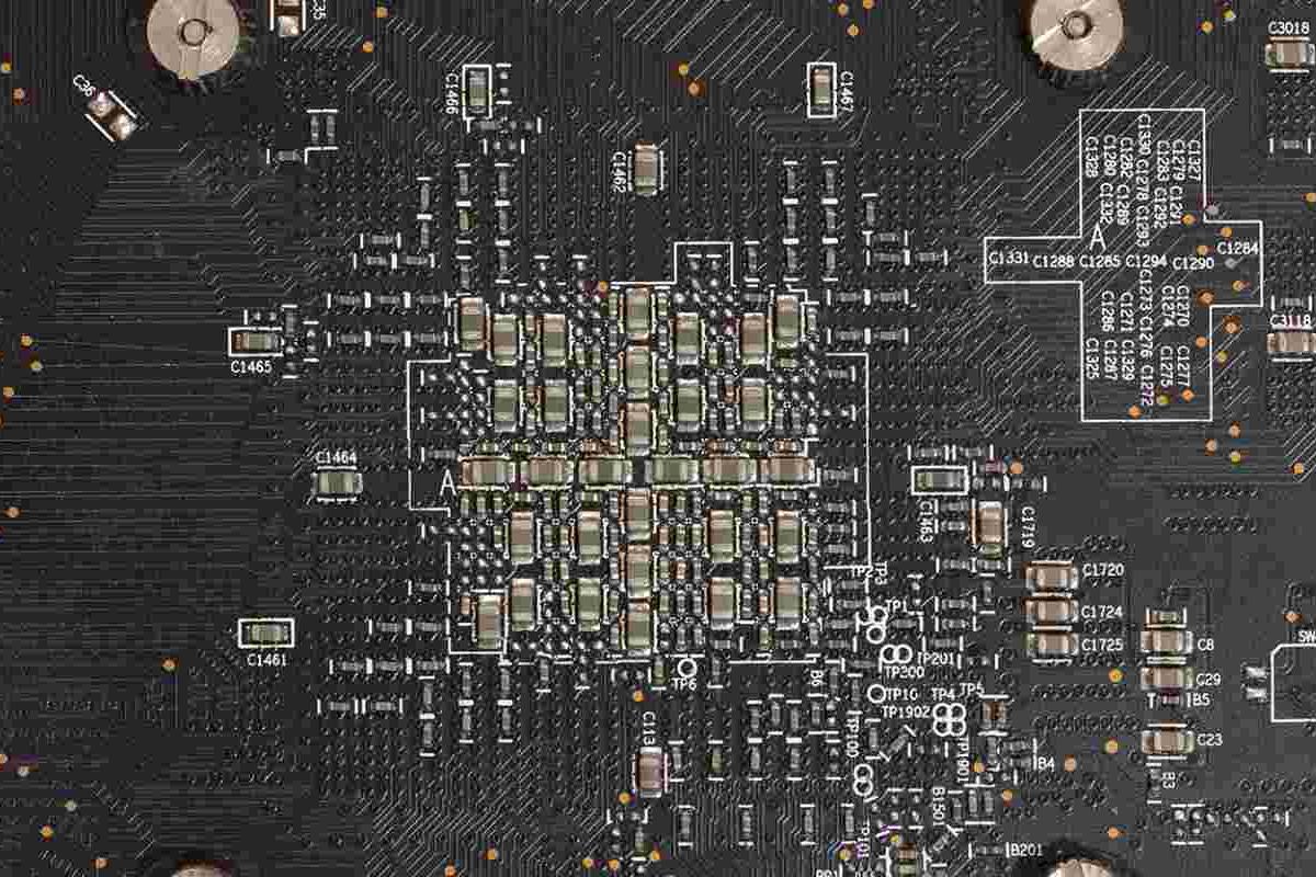
High-density PCBs are characterized by tightly packed components, narrow traces, and minimal spacing. These designs often incorporate fine pitch components, where the distance between pins is incredibly small, sometimes as low as 0.5mm or less. In such environments, every detail of the PCB manufacturing process matters. Below are the standout matte solder mask benefits that make it ideal for these complex designs.
1. Improved Inspection and Quality Control
One of the primary advantages of matte solder mask is its ability to facilitate better inspection during manufacturing and assembly. High-density PCBs often have hundreds or even thousands of tiny components and connections packed into a small area. Inspecting these boards for defects, such as misaligned solder masks or incomplete coverage, is critical to ensuring functionality.
Unlike glossy finishes, which can create glare under bright lights, matte solder mask diffuses light and reduces reflections. This non-reflective surface makes it easier for automated optical inspection (AOI) systems and human inspectors to spot issues like pinholes, uneven coatings, or misalignments. For instance, during AOI, a matte finish can improve image clarity by minimizing light scatter, leading to more accurate defect detection. This is especially valuable in high-density designs where even a minor flaw can cause a short circuit or signal interference.

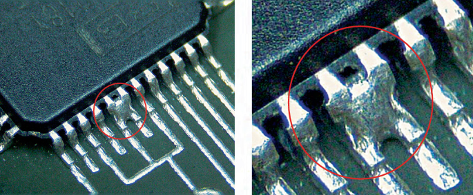
2. Solder Bridging Prevention in Fine Pitch Components
Solder bridging, where excess solder creates an unintended connection between two adjacent pads or pins, is a common issue in PCB assembly, especially with fine pitch components. In high-density PCB design, the spacing between pins can be as tight as 0.4mm, leaving little room for error during soldering. A single bridge can lead to a short circuit, rendering the board unusable.
Matte solder mask helps in solder bridging prevention by providing a surface that minimizes solder spread. The slightly rougher texture of matte finishes can reduce the likelihood of solder flowing beyond the intended pad area compared to smoother glossy finishes. Additionally, matte solder mask often pairs well with precise solder mask dams—thin strips of mask material between closely spaced pads—that further prevent solder from bridging. This combination is particularly effective for fine pitch components, ensuring clean and reliable soldering even in the most compact layouts.
Technical Insight: Studies suggest that solder mask dams as narrow as 0.1mm can effectively prevent bridging in designs with pad spacing below 0.5mm. When combined with a matte finish, the risk of solder creep is further reduced, enhancing assembly yields by up to 15% in some high-density applications.
3. Enhanced Compatibility with High-Density PCB Design
High-density PCB design often involves multilayer boards with complex routing, microvias, and tightly packed components. These designs push the limits of manufacturing tolerances, requiring materials that support precision and reliability. Matte solder mask is well-suited for such applications due to its uniform application and reduced risk of defects during the coating process.
In high-density layouts, the solder mask must adhere perfectly to narrow traces and small vias without pooling or thinning. Matte solder mask formulations are often designed to provide consistent coverage, even on intricate geometries. This ensures that the copper traces remain protected from environmental factors like moisture and dust, which could otherwise cause corrosion or signal degradation over time. For engineers working on boards with trace widths as small as 3 mils (0.076mm), this level of protection is non-negotiable.
Technical Insight: Matte solder mask can maintain dielectric strength up to 500V/mil, providing robust insulation in high-density designs where traces are closely spaced. This helps prevent electrical arcing, a common concern in compact boards operating at voltages above 5V.
4. Better Thermal and Mechanical Stability
High-density PCBs often operate in demanding environments, whether in consumer electronics exposed to frequent handling or industrial systems facing high temperatures. Matte solder mask offers improved thermal and mechanical stability compared to some glossy alternatives. Its composition can better withstand the heat of reflow soldering processes, which often reach temperatures of 260°C or higher, without cracking or peeling.
Additionally, the non-reflective surface of matte solder mask can help dissipate heat more evenly across the board, reducing the risk of localized hotspots in densely packed areas. This is particularly beneficial for PCBs with high-power components that generate significant heat during operation. Mechanically, matte finishes are less prone to scratches and wear during handling, ensuring the protective layer remains intact throughout the board’s lifecycle.
5. Aesthetic and Functional Balance
While functionality is the primary concern in PCB design, aesthetics can also play a role, especially for consumer-facing products where the PCB may be visible. Matte solder mask provides a clean, professional look with a subtle, non-shiny appearance that appeals to designers and manufacturers alike. Beyond looks, this finish reduces glare in environments where technicians or end-users interact with the board under bright lighting, aligning with the improved inspection benefits mentioned earlier.
In high-density PCB design, where every detail is scrutinized, the matte finish ensures that the focus remains on performance without distractions from reflective surfaces. This balance of form and function makes it a versatile choice for a wide range of applications, from wearable devices to automotive electronics.
Applications of Matte Solder Mask in High-Density PCB Design
Matte solder mask is particularly well-suited for industries and applications where high-density PCBs are the norm. Here are a few key areas where its benefits shine:
- Consumer Electronics: Smartphones, tablets, and wearables rely on compact, high-density PCBs with fine pitch components. Matte solder mask ensures reliable assembly and inspection in these space-constrained designs.
- Medical Devices: Precision and reliability are critical in medical electronics. Matte solder mask helps prevent solder bridging and supports stringent quality control processes.
- Automotive Systems: With the rise of electric vehicles and advanced driver-assistance systems (ADAS), automotive PCBs must handle high densities and harsh conditions. Matte solder mask provides the necessary durability and thermal stability.
- Telecommunications: High-speed communication equipment often uses multilayer PCBs with tight tolerances. Matte solder mask supports signal integrity by ensuring consistent insulation and protection.
Technical Insight: In telecommunications, high-density PCBs for 5G applications often require impedance control within ±10% of target values (e.g., 50 ohms for RF lines). Matte solder mask contributes by maintaining uniform dielectric properties, minimizing signal loss at frequencies above 1 GHz.
How to Choose the Right Solder Mask for Your High-Density PCB
While matte solder mask offers numerous advantages, it’s important to evaluate your specific project requirements before making a decision. Here are some factors to consider:
- Design Complexity: If your PCB features fine pitch components or extremely tight spacing, matte solder mask’s benefits in solder bridging prevention and inspection are highly relevant.
- Manufacturing Process: Ensure that your fabrication and assembly partners can apply matte solder mask with precision, especially for high-density designs with narrow solder mask dams.
- Operating Environment: For boards exposed to high temperatures or mechanical stress, matte solder mask’s stability can be a deciding factor.
- Inspection Needs: If your quality control process relies heavily on optical inspection, the reduced glare of matte finishes can improve accuracy and efficiency.
By aligning your solder mask choice with these considerations, you can optimize both the performance and manufacturability of your high-density PCB design.
Conclusion: Why Matte Solder Mask Is a Game-Changer for High-Density PCBs
In the realm of high-density PCB design, every decision—from material selection to surface finish—impacts the final product’s quality and reliability. Matte solder mask stands out as a powerful ally for engineers tackling complex layouts with fine pitch components. Its benefits, including improved inspection, solder bridging prevention, compatibility with tight tolerances, and enhanced stability, make it an ideal choice for modern electronics.
Whether you’re designing a compact consumer gadget or a critical industrial system, leveraging the advantages of matte solder mask can streamline your manufacturing process and boost performance. By prioritizing precision and protection, this finish helps ensure that your high-density PCBs meet the highest standards of quality and functionality.
At ALLPCB, we’re committed to supporting your PCB projects with cutting-edge solutions and expert guidance. Explore how matte solder mask can elevate your designs and bring your innovations to life with confidence.