 ALLPCB


If you're facing challenges with buried via reliability in your PCB designs, you're not alone. Buried vias, while essential for high-density interconnects, can introduce reliability issues like signal degradation, thermal stress, and manufacturing defects. This guide offers a practical approach to troubleshooting buried via PCB reliability problems, helping you identify and resolve issues effectively. Whether you're looking into buried via failure analysis, testing methods, defect detection, or ways to improve reliability, we've got you covered with actionable insights and detailed steps.
In this comprehensive post, we'll dive deep into the world of buried vias, exploring their role in modern PCB designs, common reliability issues, and proven strategies to ensure long-term performance. Let's get started on enhancing the durability and efficiency of your PCB projects.
What Are Buried Vias and Why Do They Matter in PCB Design?
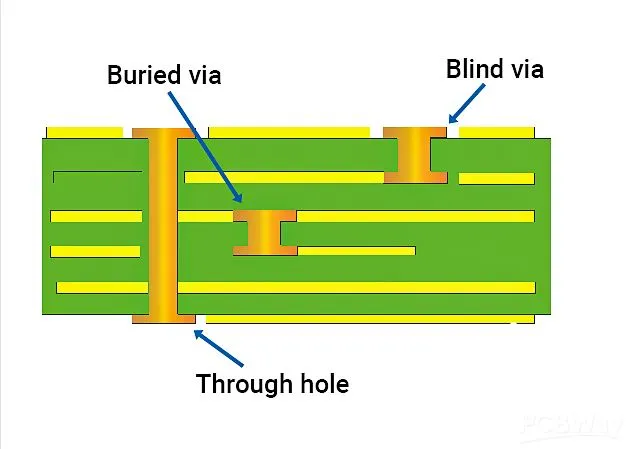
Buried vias are a type of via used in multilayer printed circuit boards (PCBs) that connect internal layers without reaching the outer surfaces. Unlike through-hole or blind vias, buried vias are completely hidden within the PCB stack-up, making them ideal for high-density designs where space is limited. They allow for more complex routing and help reduce the overall size of the board, which is critical in applications like smartphones, medical devices, and aerospace technology.
However, the hidden nature of buried vias also makes them prone to reliability issues. Since they are not accessible for direct inspection or repair, any defect or failure can be challenging to detect and fix. This is why understanding buried via PCB reliability is crucial for engineers aiming to create robust and long-lasting designs. Poorly designed or manufactured buried vias can lead to signal integrity problems, increased impedance, or even complete board failure under stress.
Common Buried Via Reliability Issues in PCBs
Before diving into troubleshooting, it's important to understand the common problems associated with buried vias. Identifying these issues early can save time and resources during the design and manufacturing process. Below are some of the most frequent challenges related to buried via PCB reliability:
- Signal Integrity Degradation: Buried vias can introduce impedance mismatches, especially in high-speed designs. For instance, a poorly designed via might cause a reflection in a signal traveling at 5 GHz, leading to data loss or errors.
- Thermal Stress: During operation or soldering, thermal expansion can stress buried vias, causing cracks or delamination. This is particularly common in boards exposed to temperature cycles between -40°C and 85°C.
- Manufacturing Defects: Issues like incomplete plating or voids in the via barrel can occur during fabrication, weakening the connection between layers. Studies show that up to 15% of PCB failures can be traced back to via-related defects.
- Mechanical Failure: Physical stress from bending or vibration can lead to fractures in buried vias, especially in flexible or rigid-flex PCBs.
Recognizing these problems is the first step in buried via failure analysis. By pinpointing the root cause, you can apply targeted solutions to prevent costly rework or product recalls.
Step-by-Step Guide to Buried Via Failure Analysis
Conducting a thorough buried via failure analysis is essential to diagnose and address reliability issues. Follow these practical steps to systematically investigate and resolve problems:
Step 1: Visual and Microscopic Inspection
Start by examining the PCB for any visible signs of damage or irregularity. While buried vias are not visible on the surface, a cross-sectional analysis using a microscope can reveal issues like cracks, voids, or improper plating. Look for discontinuities in the copper barrel or separation between layers, which indicate potential failure points.
Step 2: Electrical Testing for Continuity
Use a multimeter or automated test equipment to check for continuity across the buried vias. A resistance reading higher than expected (e.g., above 10 milliohms for a typical via) could signal a partial break or poor connection. This step helps in early buried via defect detection before the issue escalates.
Step 3: Thermal Imaging for Hotspots
Thermal imaging cameras can detect hotspots caused by high resistance in buried vias during operation. A temperature difference of more than 10°C compared to surrounding areas might indicate a defective via struggling to handle current flow.
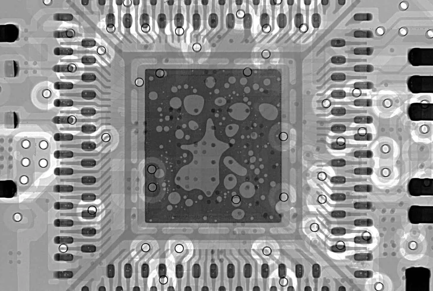
Step 4: X-Ray Inspection for Hidden Defects
For non-destructive testing, X-ray imaging is a powerful tool to inspect buried vias. It can reveal internal voids, misalignments, or incomplete fills that are not visible through other methods. This is particularly useful in high-density boards where multiple buried vias are present.
Buried Via Testing Methods to Ensure Reliability
Testing is a critical component of maintaining buried via PCB reliability. Implementing robust buried via testing methods during design validation and production can prevent failures. Here are some effective techniques to consider:
1. Design Simulation for Signal Integrity
Before manufacturing, use simulation software to model the behavior of buried vias in your PCB layout. Tools can predict impedance values (typically aiming for 50 ohms in high-speed designs) and identify potential signal reflection issues. Adjusting via dimensions or placement based on simulation results can significantly improve performance.
2. Accelerated Life Testing (ALT)
Subject your PCB to accelerated life testing under extreme conditions, such as temperature cycling from -55°C to 125°C or high humidity levels (up to 85% RH). This helps simulate years of use in a short period, revealing how buried vias hold up under stress.
3. Microsection Analysis
After manufacturing, perform a microsection analysis by cutting through a sample PCB to examine the buried vias under a high-powered microscope. This destructive testing method can confirm if the vias meet design specifications, such as a minimum wall thickness of 25 micrometers for reliable plating.
4. In-Circuit Testing (ICT)
During production, use in-circuit testing to verify the electrical performance of buried vias. ICT can detect open circuits or shorts, ensuring that each via functions as intended before the board is assembled into a final product.
By integrating these buried via testing methods into your workflow, you can catch issues early and maintain high reliability standards for your PCB designs.
Buried Via Defect Detection: Tools and Techniques
Effective buried via defect detection requires a combination of advanced tools and careful techniques. Since buried vias are not accessible on the surface, specialized methods are needed to identify problems without damaging the board. Here are some proven approaches:
- Automated Optical Inspection (AOI): While AOI is primarily used for surface defects, advanced systems with 3D capabilities can sometimes detect alignment issues that affect buried vias. This is useful during the early stages of manufacturing.
- Computed Tomography (CT) Scanning: For a detailed 3D view of internal structures, CT scanning provides unparalleled insight into buried via integrity. It can identify micro-cracks or plating inconsistencies with precision.
- Time-Domain Reflectometry (TDR): TDR is a non-destructive testing method that measures signal reflections to locate impedance discontinuities caused by defective buried vias. It's especially valuable for high-speed PCB designs.
Using these tools for buried via defect detection ensures that even the smallest issues are identified before they lead to larger failures, saving time and cost in the long run.
Strategies for Improving Buried Via Reliability
Prevention is always better than repair when it comes to buried via reliability. By focusing on design and manufacturing best practices, you can minimize the risk of failures. Here are actionable strategies for improving buried via reliability:
1. Optimize Via Design Parameters
Design buried vias with appropriate dimensions to match your application. For example, a via diameter of 0.2 mm with an aspect ratio (depth-to-diameter) of less than 10:1 is generally considered reliable for most multilayer boards. Avoid overly small vias that are difficult to plate uniformly.
2. Use High-Quality Materials
Select PCB materials with low coefficients of thermal expansion (CTE) to reduce stress on buried vias during temperature changes. Materials with a CTE below 15 ppm/°C are often recommended for high-reliability applications.
3. Implement Robust Manufacturing Processes
Work with manufacturers who follow strict process controls, such as sequential lamination for multilayer boards. Ensure that via drilling and plating processes are optimized to avoid defects like voids or thin copper walls.
4. Incorporate Redundancy in Critical Connections
For mission-critical applications, consider adding redundant buried vias to ensure connectivity even if one via fails. This can be a lifesaver in aerospace or medical devices where reliability is non-negotiable.
5. Regular Reliability Testing
Schedule periodic testing during the product lifecycle to monitor buried via performance. Environmental stress screening (ESS) with vibration and thermal cycling can help identify weak points before they cause field failures.
By adopting these strategies, you can significantly enhance the durability of your PCBs and achieve long-term success in improving buried via reliability.
Conclusion: Building Reliable PCBs with Buried Vias
Buried vias are a cornerstone of modern PCB design, enabling compact and complex layouts for advanced electronics. However, their hidden nature makes them susceptible to reliability issues that can compromise the performance of your boards. Through effective buried via failure analysis, testing methods, and defect detection techniques, you can troubleshoot and resolve problems before they escalate. Moreover, by focusing on design optimization and manufacturing best practices, improving buried via reliability becomes an achievable goal.
This practical guide has walked you through the key aspects of managing buried via PCB reliability, from identifying common issues to implementing robust solutions. Armed with these insights, you can confidently tackle challenges and ensure your PCB designs stand the test of time. Keep these strategies in mind during your next project to create reliable, high-performing boards that meet the demands of today's technology.


