 ALLPCB


If you're looking for a reliable and widely used solution for protecting your printed circuit boards (PCBs), green solder mask is the go-to choice for many designers and manufacturers. But what makes it so popular? Green solder mask offers excellent protection against oxidation, prevents solder bridges, and enhances the durability of PCBs, all while being cost-effective and visually clear for inspections. In this comprehensive guide, we'll dive deep into the advantages, properties, applications, and best practices for using green solder mask in PCB design and manufacturing. Whether you're an engineer, designer, or hobbyist, this article will provide actionable insights to help you make informed decisions.
What Is Green Solder Mask and Why Does It Matter?
A solder mask is a thin, protective layer applied to the copper traces of a PCB to prevent oxidation, avoid unintended solder connections, and insulate the board's conductive paths. Traditionally, this layer comes in green, which has become the industry standard due to its historical use and practical benefits. The green color isn’t just for aesthetics—it plays a functional role in manufacturing and inspection processes.
Understanding the role of green solder mask is crucial for anyone involved in PCB design or production. It directly impacts the reliability, longevity, and performance of electronic devices. In the sections below, we'll explore why green solder mask stands out, its specific properties, and how to apply it effectively in your projects.

Green Solder Mask Advantages: Why Choose Green?
The popularity of green solder mask isn’t accidental. It offers several distinct benefits that make it a preferred choice for PCB designers and manufacturers worldwide. Let’s break down the key advantages:
- Cost-Effectiveness: Green solder mask materials are widely available and have been used for decades, making them more affordable compared to other colors or specialized coatings. This keeps production costs low, especially for large-scale manufacturing.
- High Contrast for Inspection: The green color provides excellent contrast against white silkscreen markings and copper traces, making it easier to spot defects or misalignments during visual inspections. This can reduce errors in quality control processes by up to 30%, according to industry studies.
- Proven Reliability: Green solder mask formulations have been refined over years of use, offering consistent protection against environmental factors like humidity and temperature fluctuations. This reliability is critical for applications in consumer electronics, automotive, and industrial sectors.
- Compatibility with Processes: Most PCB manufacturing equipment and processes are optimized for green solder mask, ensuring smooth application and minimal risk of errors during production.
- Standardization: Since green is the industry standard, using it ensures compatibility with existing design libraries, software tools, and manufacturing workflows, saving time and effort in the design phase.
These advantages make green solder mask a practical choice for most PCB projects, balancing performance with cost. However, understanding its properties is just as important to ensure it meets your specific needs.
Green Solder Mask Properties: What Makes It Effective?
The effectiveness of green solder mask comes down to its physical and chemical properties, which are tailored to protect PCBs under various conditions. Here are the key properties that define its performance:
- Chemical Resistance: Green solder mask, often made from epoxy-based or liquid photoimageable (LPI) materials, resists harsh chemicals used during soldering and cleaning processes. This prevents degradation over time, even in aggressive environments.
- Thermal Stability: It can withstand high temperatures during reflow soldering, typically up to 260°C for short durations, without breaking down or losing its protective qualities. This makes it suitable for both leaded and lead-free soldering processes.
- Electrical Insulation: With a dielectric strength often exceeding 500V per mil (0.001 inch), green solder mask provides robust insulation between closely spaced copper traces, preventing short circuits and ensuring signal integrity.
- Durability: The material is resistant to mechanical stress, such as scratches or abrasion during handling, which helps maintain the integrity of the PCB throughout its lifecycle.
- Adhesion: Green solder mask adheres strongly to the PCB substrate and copper traces, ensuring it doesn’t peel or crack under thermal or mechanical stress.
These properties make green solder mask a versatile and reliable choice for protecting PCBs across different applications. But how do you apply it effectively in design and manufacturing? Let’s explore that next.
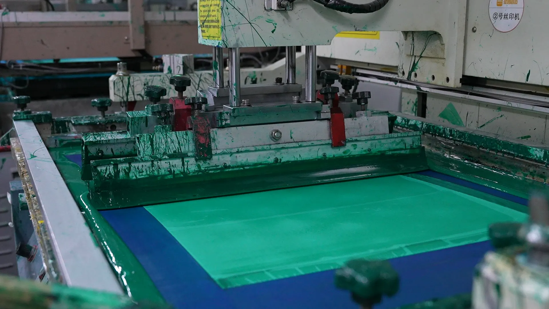
Green Solder Mask Application Guide: Steps for Success
Applying green solder mask correctly is critical to achieving the desired protection and performance for your PCB. Whether you're a designer or manufacturer, following a structured process ensures optimal results. Below is a step-by-step guide to applying green solder mask:
- Surface Preparation: Start by cleaning the PCB surface to remove any contaminants like dust, grease, or oxidation. A clean surface ensures proper adhesion of the solder mask. Use a chemical cleaner or micro-etching process for best results.
- Mask Application: Depending on the type of solder mask (liquid photoimageable or dry film), apply the material evenly across the PCB surface. For LPI masks, use screen printing or spray coating to achieve a uniform layer, typically 0.8 to 1.2 mils thick.
- Exposure and Development: For photoimageable masks, expose the layer to UV light through a photomask to define areas where components will be soldered. Unexposed areas are then removed during the development process using a chemical developer, leaving openings for solder pads.
- Curing: Cure the solder mask by baking the PCB at a controlled temperature (typically 120-150°C for 30-60 minutes). This hardens the mask, enhancing its durability and chemical resistance.
- Inspection: After curing, inspect the board for defects such as pinholes, uneven coverage, or misalignment. Use automated optical inspection (AOI) systems to ensure precision, especially for high-density designs.
Following these steps minimizes the risk of issues like solder mask peeling or insufficient coverage, which can compromise the PCB's performance. For complex designs, consult with your manufacturing partner to adjust parameters like curing time or mask thickness based on specific requirements.
Green Solder Mask PCB Design: Tips for Optimal Results
Designing a PCB with green solder mask in mind can significantly improve manufacturing outcomes and board reliability. Here are some practical tips to consider during the design phase:
- Solder Mask Clearance: Ensure a minimum clearance of 0.1 mm (4 mils) between the solder mask edge and the copper pad to prevent mask overlap, which can interfere with soldering. For high-density designs, tighter clearances may be needed, so verify with your manufacturer.
- Via Tenting: Decide whether vias should be tented (covered with solder mask) or left open. Tenting protects vias from environmental exposure but may trap moisture if not done correctly. For most applications, tenting is recommended to reduce corrosion risks.
- Pad Coverage: Avoid excessive solder mask on pads, as it can lead to poor solder joints. Use software tools to define precise openings (solder mask relief) around pads, typically 0.05-0.1 mm larger than the pad size.
- Trace Spacing: Maintain adequate spacing between traces to allow for solder mask application without bridging. A minimum spacing of 0.15 mm (6 mils) is often recommended for standard designs to ensure insulation.
- Design for Inspection: Leverage the high contrast of green solder mask by placing silkscreen markings strategically for easy readability during quality checks. This can speed up troubleshooting and assembly processes.
By incorporating these design considerations, you can avoid common pitfalls and ensure your PCB performs reliably after manufacturing. Collaboration with your fabrication team early in the design process can further optimize these parameters.

Green Solder Mask Manufacturing: Best Practices
Manufacturing PCBs with green solder mask requires attention to detail to achieve consistent quality. Here are some best practices to follow during production:
- Material Selection: Choose a high-quality green solder mask material that matches your application needs. Liquid photoimageable (LPI) masks are ideal for fine-pitch designs, while epoxy-based masks offer better chemical resistance for harsh environments.
- Process Control: Maintain strict control over application parameters like coating thickness, exposure time, and curing temperature. Variations can lead to defects like bubbles or incomplete curing, which compromise protection.
- Environmental Conditions: Apply solder mask in a clean, controlled environment to avoid contamination. Dust or humidity levels above 60% can cause adhesion issues or surface defects.
- Testing and Validation: After application, conduct tests like adhesion testing (using tape tests per IPC standards) and thermal shock testing to verify the solder mask’s performance under stress. This ensures reliability in real-world conditions.
- Feedback Loop: Work closely with your design team to address any issues identified during manufacturing. Continuous feedback helps refine future designs and processes for better outcomes.
Implementing these best practices during manufacturing can reduce defect rates by as much as 20%, based on industry benchmarks, leading to higher yields and lower costs.
Applications of Green Solder Mask in Various Industries
Green solder mask is used across a wide range of industries due to its versatility and proven performance. Here are some common applications where it plays a critical role:
- Consumer Electronics: From smartphones to laptops, green solder mask protects the intricate circuits in everyday devices, ensuring reliability under frequent use and varying conditions.
- Automotive: In automotive electronics, such as engine control units (ECUs), green solder mask withstands high temperatures and vibrations, contributing to vehicle safety and performance.
- Industrial Equipment: For control systems and machinery, green solder mask provides durability against harsh environments, including exposure to chemicals and moisture.
- Medical Devices: In critical applications like diagnostic equipment, the insulation and protection offered by green solder mask ensure consistent operation and patient safety.
- Aerospace: Green solder mask is used in avionics and satellite systems, where reliability under extreme conditions (temperature swings from -40°C to 85°C) is non-negotiable.
These diverse applications highlight the adaptability of green solder mask, making it a trusted solution for both standard and specialized PCB needs.

Conclusion: Maximizing the Value of Green Solder Mask
Green solder mask remains a cornerstone of PCB design and manufacturing due to its cost-effectiveness, reliability, and ease of use. By understanding its advantages, properties, and best practices for application, you can ensure your PCBs are well-protected and perform optimally in any environment. Whether you're designing for consumer gadgets or industrial systems, following the guidelines for green solder mask in PCB design and manufacturing will help you achieve consistent, high-quality results.
At ALLPCB, we’re committed to supporting your projects with top-tier manufacturing solutions and expert guidance. By leveraging the benefits of green solder mask, you can enhance the durability and functionality of your PCBs while keeping costs in check. Use this guide as a roadmap to integrate green solder mask effectively into your next project, and experience the difference it makes firsthand.


