 ALLPCB


In the realm of space exploration, every gram and centimeter counts. Space probes, tasked with venturing into the unknown, must carry advanced electronics in the smallest possible footprint while maintaining top-tier performance. This is where the miniaturization of Printed Circuit Boards (PCBs) for space probes comes into play. How do engineers achieve high-density PCB design for space probes, and what are the best practices for space probe PCB component miniaturization? In this blog, we dive deep into the world of compact PCB layout techniques for space applications and explore how miniaturized space probe electronics are designed to balance size with uncompromised functionality.
Whether you're an engineer working on aerospace projects or simply curious about the technology behind space missions, this guide will walk you through the challenges, techniques, and innovations driving the miniaturization of space probe PCBs. Let’s explore how these tiny yet powerful boards are engineered to survive the harsh conditions of space while delivering critical data back to Earth.
Why Miniaturization Matters in Space Probe Electronics
Space probes operate in an environment where size, weight, and power efficiency are non-negotiable constraints. Every component on a probe must justify its inclusion by offering maximum functionality in the smallest package. Miniaturized space probe electronics allow for more instruments to be packed into a limited space, enabling probes to conduct a wider range of scientific experiments. Additionally, smaller and lighter PCBs reduce launch costs, as weight directly impacts fuel requirements.
Beyond cost and space savings, miniaturization enhances reliability. With fewer materials exposed to the extreme conditions of space—such as radiation, temperature swings, and vacuum—there are fewer points of potential failure. However, shrinking PCB designs introduces complex challenges in maintaining signal integrity, thermal management, and durability. Let’s break down these challenges and the solutions that make high-density PCB design for space probes possible.

Key Challenges in Space Probe PCB Component Miniaturization
Designing PCBs for space probes isn’t just about making them smaller. Engineers must address several unique hurdles to ensure these boards perform reliably in the harshest environments imaginable. Here are the primary challenges:
1. Harsh Environmental Conditions
Space is an unforgiving place. PCBs in space probes face extreme temperatures ranging from -150°C to 125°C, high levels of radiation, and the vacuum of space that prevents traditional heat dissipation through convection. These conditions can degrade materials, disrupt signal integrity, and cause mechanical stress on tiny components. Miniaturized designs must use materials and layouts that withstand these factors without compromising performance.
2. Signal Integrity in High-Density Designs
As components are packed closer together in high-density PCB designs for space probes, the risk of electromagnetic interference (EMI) and crosstalk increases. Maintaining signal integrity is critical, especially when dealing with high-speed data transmission rates often required for real-time communication with Earth. For instance, signal speeds in modern space probe systems can exceed 1 Gbps, requiring precise impedance matching (typically around 50 ohms for RF signals) to avoid data loss or corruption.
3. Power and Thermal Management
Smaller PCBs mean less surface area for heat dissipation, yet space probes often rely on power-intensive instruments. Overheating can lead to component failure, so engineers must incorporate efficient thermal vias, heat sinks, and sometimes active cooling systems within a compact design. Balancing power efficiency with thermal management is a constant struggle in miniaturized space probe electronics.
4. Limited Physical Space
Space probes are often constrained by strict size limits. For example, CubeSats, a popular class of small satellites, adhere to a standard size of 10 cm x 10 cm x 10 cm per unit. Fitting all necessary electronics into such a confined space requires innovative compact PCB layout techniques for space applications, often involving multi-layer boards and micro-components.
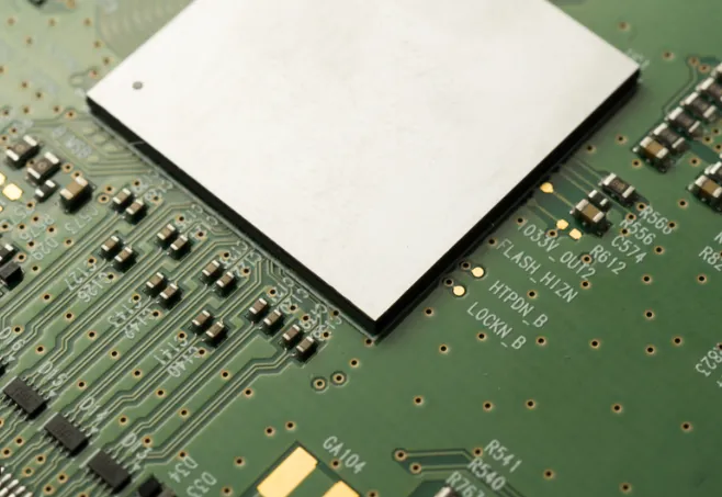
Techniques for Compact PCB Layout in Space Probes
To overcome the challenges of miniaturization, engineers employ a variety of advanced techniques. These methods ensure that space probe PCB component miniaturization doesn’t come at the cost of performance or reliability. Below are some of the most effective strategies for achieving compact, high-density designs.
1. Multi-Layer PCB Designs
One of the most common approaches to high-density PCB design for space probes is the use of multi-layer boards. By stacking multiple layers of circuitry, engineers can fit more components and traces into a smaller footprint. A typical space probe PCB might have 8 to 16 layers, allowing for complex routing while minimizing the board’s surface area. However, multi-layer designs require precise alignment and insulation between layers to prevent shorts and interference.
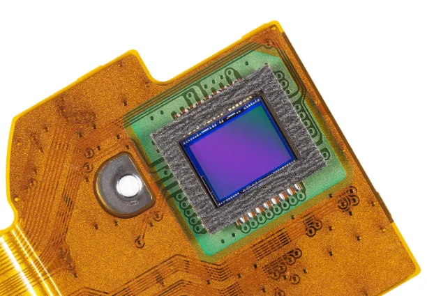
2. Surface Mount Technology (SMT)
Surface Mount Technology has revolutionized PCB miniaturization by allowing components to be mounted directly onto the board’s surface rather than through holes. SMT components, such as resistors and capacitors, can be as small as 0.4 mm x 0.2 mm (0402 package size), enabling incredible density. This technique is essential for miniaturized space probe electronics, where every millimeter matters.
3. High-Density Interconnect (HDI) Technology
HDI technology takes multi-layer designs to the next level by using microvias (vias with diameters less than 0.15 mm) and finer traces (often below 0.1 mm in width). This allows for even tighter packing of components and connections, making HDI a go-to solution for compact PCB layout techniques in space applications. HDI boards also improve signal integrity by reducing the length of signal paths, which is critical for high-speed data transmission.
4. Component Miniaturization
Advances in microelectronics have led to smaller, more efficient components tailored for space use. For example, microcontrollers and sensors designed for aerospace applications now come in packages smaller than 1 mm2 while offering robust performance. Selecting the right miniaturized components is a key step in space probe PCB component miniaturization, ensuring that functionality isn’t sacrificed for size.
5. 3D Packaging and Chip-on-Board (CoB) Technology
In extreme space-constrained designs, engineers turn to 3D packaging, where components are stacked vertically or integrated directly onto the board without traditional packaging (as in Chip-on-Board designs). These methods drastically reduce the PCB’s footprint and are often used in CubeSats and other small space probes to maximize space efficiency.
Image Placement Suggestion: Include an image here of a 3D-packaged PCB or Chip-on-Board design used in a space application. ALT Text: "3D packaging in space probe PCB for compact electronics design."
Material Selection for Miniaturized Space Probe Electronics
The materials used in space probe PCBs play a crucial role in their performance and durability. Standard materials like FR-4, commonly used in consumer electronics, often fall short in space due to their limited thermal and radiation resistance. Instead, engineers opt for specialized materials suited for the unique demands of space.
1. Polyimide Substrates
Polyimide is a popular choice for space probe PCBs due to its excellent thermal stability (withstanding temperatures from -200°C to 300°C) and resistance to radiation. Its flexibility also allows for the creation of rigid-flex boards, which can be folded or shaped to fit into tight spaces, further aiding miniaturization.
2. Ceramic-Based Materials
For applications requiring even higher thermal and mechanical stability, ceramic substrates are used. These materials can handle extreme conditions and provide better heat dissipation, though they are more expensive and harder to manufacture. Ceramic PCBs are often found in critical systems of space probes where reliability is paramount.
3. Radiation-Hardened Components
In addition to substrate materials, the electronic components themselves must be radiation-hardened. Radiation can cause bit flips in memory or damage to semiconductors, so components are often designed or shielded to withstand doses up to 100 krad (a unit of absorbed radiation). Using rad-hard components is essential for ensuring the longevity of miniaturized space probe electronics.
Balancing Size and Performance: Best Practices
Achieving the perfect balance between size and performance in space probe PCBs requires a combination of innovative design, careful planning, and rigorous testing. Here are some best practices to guide engineers in creating effective miniaturized designs.
1. Prioritize Critical Functions
Not all systems on a space probe are equally important. Engineers must prioritize critical functions—such as communication and navigation—when allocating space and resources on the PCB. Less critical systems can often use shared or multi-purpose components to save space.
2. Optimize Power Consumption
Power efficiency is vital in space, where energy sources like solar panels provide limited output. Using low-power components and designing efficient power distribution networks (often with voltages as low as 1.8V for digital circuits) helps extend the probe’s operational life while reducing heat generation.
3. Simulate and Test Extensively
Before a space probe launches, its electronics must undergo extensive simulation and testing to ensure they can handle the stresses of space. Tools like thermal modeling software and radiation testing chambers help engineers identify potential weaknesses in high-density PCB designs for space probes, allowing for adjustments before deployment.
4. Collaborate Across Disciplines
PCB miniaturization for space probes isn’t just an electrical engineering challenge—it requires input from mechanical engineers, thermal experts, and materials scientists. A collaborative approach ensures that all aspects of the design, from size to durability, are optimized for the mission’s goals.
Future Trends in Space Probe PCB Miniaturization
The field of miniaturized space probe electronics is constantly evolving, driven by advancements in technology and the growing demand for smaller, more capable spacecraft. Here are a few trends to watch in the coming years.
1. Increased Use of AI in Design
Artificial Intelligence (AI) is beginning to play a role in PCB design by automating layout optimization and identifying potential issues in high-density designs. AI tools can analyze millions of design configurations to find the most space-efficient and reliable solution, saving engineers time and resources.
2. Advanced Materials
Research into new materials, such as graphene-based substrates, promises to further enhance the performance of space probe PCBs. These materials could offer superior conductivity and heat dissipation in even smaller packages, pushing the boundaries of miniaturization.
3. Modular and Reusable Designs
As space missions become more frequent, there’s a growing emphasis on modular PCB designs that can be reused or adapted for different probes. This approach reduces costs and speeds up development while maintaining the benefits of compact layouts.
Conclusion: The Art of Miniaturization in Space Exploration
The miniaturization of space probe PCBs is a remarkable feat of engineering that balances the competing demands of size, performance, and reliability. Through techniques like multi-layer designs, HDI technology, and the use of advanced materials, engineers create compact PCB layouts for space applications that power humanity’s quest to explore the cosmos. As technology advances, the future of miniaturized space probe electronics looks brighter than ever, promising even smaller, more powerful systems for the next generation of space missions.
At ALLPCB, we’re proud to support the aerospace industry by providing high-quality PCB manufacturing solutions tailored to the unique needs of space exploration. Whether you’re working on high-density PCB designs for space probes or other cutting-edge projects, our expertise and commitment to precision can help bring your ideas to life. Let’s push the boundaries of what’s possible—together.


