 ALLPCB


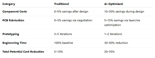
In the fast-paced world of electronics, reducing costs in PCB design without sacrificing quality is a top priority for engineers and manufacturers. By leveraging AI for efficient resource allocation, you can achieve significant savings and streamline the design process. This blog explores how AI-driven tools and strategies can optimize PCB design, cut expenses, and improve overall efficiency. Whether you're looking for ways to lower production costs or enhance design precision, AI offers powerful solutions for AI PCB cost reduction, efficient PCB design, and PCB design optimization.
Why Cost Reduction in PCB Design Matters
Printed Circuit Boards (PCBs) are the backbone of modern electronics, found in everything from smartphones to industrial machinery. However, designing and manufacturing PCBs can be expensive due to material costs, labor, and the complexity of layouts. Reducing these costs while maintaining high performance is crucial for staying competitive in the market.
Traditional PCB design methods often involve manual processes that are time-consuming and prone to errors. These inefficiencies lead to wasted resources, higher expenses, and delayed production timelines. By integrating AI into the design process, companies can address these challenges through smarter resource allocation AI strategies, ultimately saving time and money.
How AI Transforms PCB Design for Cost Reduction
AI technology is revolutionizing the way PCBs are designed by automating repetitive tasks, predicting potential issues, and optimizing layouts. Here’s how AI contributes to AI PCB cost reduction and better resource management:
1. Automated Component Placement for Efficiency
One of the most time-intensive parts of PCB design is determining the optimal placement of components. Incorrect placement can lead to signal interference, increased manufacturing costs, and longer production times. AI algorithms analyze design requirements and automatically suggest the best component layouts to minimize issues like crosstalk or impedance mismatches.
For example, AI tools can ensure that high-speed signal components are placed closer to their respective connectors, reducing signal delay. Studies suggest that AI-driven placement can reduce signal path lengths by up to 20%, which not only improves performance but also lowers material usage and costs.
2. Intelligent Routing to Minimize Errors
Routing, or the process of connecting components on a PCB, is another area where AI shines. Manual routing often results in inefficient paths, leading to higher material costs and potential signal integrity issues. AI-powered tools can generate optimized routing paths that use the least amount of copper while maintaining electrical performance.
By reducing the length of traces, AI can cut down on material costs significantly. For instance, shorter traces might save a few cents per board, but for large-scale production runs of thousands of units, this can add up to substantial savings. Additionally, AI minimizes routing errors, reducing the need for costly redesigns.
3. Predictive Analysis for Costly Mistakes
AI doesn’t just optimize designs; it also predicts potential problems before they occur. By analyzing historical data and design parameters, AI can flag issues like thermal hotspots or areas prone to signal interference. For instance, if a design shows a high risk of overheating in a specific section, AI tools can suggest alternative layouts or materials to address the problem.
This predictive capability is a game-changer for PCB design optimization. Catching issues early prevents expensive revisions and manufacturing delays. Some AI platforms report a reduction in design errors by up to 30%, translating to fewer prototype iterations and lower overall project costs.
Efficient PCB Design with AI-Driven Resource Allocation
Resource allocation in PCB design refers to how time, materials, and manpower are distributed throughout the design and manufacturing process. Poor resource allocation leads to wasted materials, extended timelines, and higher labor costs. AI helps tackle these inefficiencies by providing data-driven insights for better decision-making.
1. Material Optimization for Lower Costs
Materials like copper, substrates, and solder masks make up a significant portion of PCB production costs. AI tools analyze design requirements to recommend the most cost-effective materials without compromising quality. For example, AI might suggest using a thinner substrate for low-power applications, reducing material expenses by 10-15% per board.
Additionally, AI minimizes material waste by optimizing the layout to fit more boards on a single panel during manufacturing. This efficient use of resources directly contributes to AI PCB cost reduction and aligns with sustainable manufacturing practices.
2. Time Savings Through Automation
Time is money in the electronics industry. The faster a design moves from concept to production, the sooner a product can reach the market. AI automates many aspects of PCB design, such as schematic checks and design rule validations, which traditionally take hours or even days when done manually.
For instance, AI can complete design rule checks (DRC) in minutes, ensuring that spacing, trace widths, and other parameters meet manufacturing standards. This automation can cut design time by up to 40%, allowing engineers to focus on innovation rather than repetitive tasks.
3. Labor Cost Reduction with AI Tools
Highly skilled engineers are essential for PCB design, but their time is valuable. AI reduces the need for manual intervention by handling routine tasks, allowing engineers to focus on complex challenges. This shift not only lowers labor costs but also improves job satisfaction by eliminating tedious work.
By incorporating AI into the workflow, companies can reduce the number of hours spent on each project. For example, a design that might take 50 hours manually could be completed in 30 hours with AI assistance, resulting in significant cost savings over multiple projects.
Key Benefits of Using AI for PCB Design Optimization
Integrating AI into PCB design offers several advantages beyond just cost reduction. These benefits make AI an indispensable tool for modern electronics development, especially when focusing on efficient PCB design and resource allocation AI.
- Improved Design Accuracy: AI ensures that designs meet performance standards by minimizing human error. For instance, it can maintain impedance values within tight tolerances, such as 50 ohms for high-speed signals, ensuring reliable operation.
- Faster Time-to-Market: With AI handling repetitive tasks, products move from design to production more quickly, giving companies a competitive edge.
- Scalability: AI tools can handle designs of varying complexity, from simple single-layer boards to intricate multi-layer designs, making them suitable for projects of any size.
- Sustainability: By reducing material waste and optimizing energy use in manufacturing, AI contributes to greener practices in electronics production.
Practical Steps to Implement AI in Your PCB Design Process
Ready to harness the power of AI for PCB design optimization? Follow these actionable steps to integrate AI into your workflow and achieve cost savings:
- Choose the Right AI Tools: Look for software platforms that offer features like automated routing, component placement, and predictive analysis. Ensure the tool integrates seamlessly with your existing design environment.
- Train Your Team: Provide training to ensure your engineers understand how to use AI tools effectively. Focus on how AI can complement their skills rather than replace them.
- Start Small: Begin with a pilot project to test AI capabilities on a smaller scale. Analyze the results to see how much time and cost savings are achieved before scaling up.
- Monitor and Adjust: Continuously evaluate the performance of AI tools in your design process. Use data from each project to fine-tune settings for maximum efficiency.

Challenges to Consider When Adopting AI for PCB Design
While AI offers numerous benefits, there are some challenges to keep in mind when adopting it for AI PCB cost reduction and design optimization:
- Initial Investment: AI software and training can be expensive upfront, though the long-term savings often outweigh the costs.
- Learning Curve: Transitioning to AI-driven workflows may require time for teams to adapt to new tools and processes.
- Data Dependency: AI relies on accurate data inputs. Poor-quality data can lead to suboptimal design suggestions, so maintaining clean and reliable data is essential.
Despite these challenges, the potential for cost savings and efficiency gains makes AI a worthwhile investment for most PCB design projects.
Future of AI in PCB Design and Cost Reduction
The role of AI in PCB design is only set to grow. As technology advances, we can expect even more sophisticated tools that further enhance efficient PCB design. For instance, future AI systems might integrate real-time manufacturing feedback to adjust designs on the fly, minimizing production errors.
Moreover, as AI becomes more accessible, small and medium-sized businesses will also be able to leverage these tools, leveling the playing field in the electronics industry. The focus on resource allocation AI will continue to drive innovation, making PCB design faster, cheaper, and more sustainable.
Conclusion: Embrace AI for Smarter PCB Design
Cost reduction in PCB design is no longer just a goal—it’s a necessity for staying competitive. By leveraging AI for PCB design optimization, companies can achieve significant savings through automated processes, intelligent resource allocation, and error prevention. From optimizing material use to slashing design time, AI offers practical solutions for AI PCB cost reduction and efficient PCB design.
At ALLPCB, we’re committed to helping you navigate the future of electronics design with cutting-edge tools and support. By embracing AI, you can streamline your workflow, reduce expenses, and bring high-quality products to market faster. Start exploring AI-driven design solutions today and see the difference in your next project.


