 ALLPCB


For startups in the electric vehicle (EV) industry, creating cost-effective battery management systems (BMS) is crucial. Battery management PCBs (printed circuit boards) are at the heart of these systems, ensuring safety, efficiency, and longevity of EV batteries. However, manufacturing these PCBs can be expensive, especially for startups with limited budgets. So, how can startups achieve high-quality PCB manufacturing while keeping costs low? The answer lies in adopting cost-effective techniques tailored for prototype PCB development, low volume production, and optimized assembly processes like surface mount assembly, reflow soldering, and automated optical inspection.
In this guide, we’ll explore practical strategies to help startups reduce expenses without compromising on quality. From choosing the right manufacturing partners to leveraging automation for cost optimization, this blog will walk you through every step of the process. Whether you’re designing your first EV battery management PCB or scaling up for small-batch production, these tips will help you save money and time.
Why Cost Optimization Matters for EV Battery Management PCBs
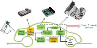
EV battery management systems are complex, requiring precise monitoring of voltage, temperature, and current across multiple battery cells. The PCB in a BMS acts as the central hub for these functions, making its design and manufacturing quality critical. For startups, balancing performance with affordability is a challenge. High costs in PCB manufacturing, especially during the prototype phase, can drain resources before a product even reaches the market.
Cost optimization in PCB production doesn’t mean cutting corners. Instead, it involves smart decisions—like selecting the right materials, streamlining designs, and using efficient assembly methods such as surface mount assembly or wave soldering. By focusing on these areas, startups can reduce expenses while maintaining the reliability needed for EV applications. Let’s dive into specific techniques that can help achieve this balance.
1. Simplify PCB Design for Cost-Effective Manufacturing
The foundation of cost-effective PCB manufacturing starts with the design phase. A well-thought-out design can significantly lower production costs, especially for prototype PCBs and low volume production. Here are some actionable tips:
- Minimize Layer Count: Each additional layer in a PCB increases manufacturing costs. For EV battery management systems, aim for a design with the fewest layers possible while meeting performance needs. A 2-layer or 4-layer board often suffices for basic BMS functions, costing 30-50% less than a 6-layer or higher design.
- Use Standard Components: Opt for widely available components with standard footprints. Custom or rare components can drive up costs due to sourcing challenges and longer lead times. For instance, using standard resistors and capacitors in surface mount assembly can save up to 20% on component costs.
- Optimize Board Size: Smaller PCBs are cheaper to produce. Design your BMS PCB to fit within standard panel sizes (like 18x24 inches) to avoid wasted material and additional fabrication fees. Reducing board size by just 10% can lower costs by 5-15%.
2. Focus on Prototype PCB Development for Early Cost Savings
Prototyping is a critical step for startups. It allows you to test and refine your EV battery management PCB before committing to full-scale production. However, prototype PCB development can be expensive if not approached strategically. Here’s how to keep costs down:
- Work with a Reliable Manufacturer: Partner with a PCB manufacturer that offers affordable prototyping services with quick turnaround times. Look for providers who can produce small batches (1-10 units) without charging high setup fees.
- Leverage Design for Manufacturability (DFM) Tools: Many manufacturers provide free DFM analysis during the prototype phase. These tools identify design issues that could lead to costly errors, such as improper trace widths or insufficient clearances. For BMS PCBs, maintaining trace widths of at least 6 mils for current-carrying paths ensures reliability without extra costs.
- Order in Small Batches: Instead of producing a large number of prototypes upfront, start with a minimal quantity. This approach limits expenses if redesigns are needed after testing. For example, ordering 5 prototype PCBs instead of 20 can cut initial costs by 75%.
3. Choose Low Volume Production for Scalable Cost Management
Once your prototype is finalized, transitioning to low volume production is the next step. This phase is ideal for startups producing small batches (100-1,000 units) to test the market or supply early customers. Here’s how to optimize costs during low volume production:
- Negotiate with Manufacturers: Many PCB manufacturers offer discounts for low volume orders if you commit to future production. Building a long-term relationship can save 10-20% on per-unit costs.
- Use Panelization: Combine multiple PCB designs onto a single panel during fabrication. This reduces material waste and lowers costs by up to 15%. For instance, panelizing 10 small BMS PCBs on one sheet can be more economical than producing them individually.
- Stick to Standard Materials: Use standard FR-4 material for your PCB substrate unless high thermal resistance or specific dielectric properties are required. FR-4 boards are 20-30% cheaper than specialized materials like Rogers or polyimide, making them ideal for cost-sensitive startups.
4. Leverage Surface Mount Assembly for Efficiency
Surface mount assembly (SMA) is a widely used technique for placing components directly onto the surface of a PCB. It’s faster and more cost-effective than through-hole assembly, especially for compact EV battery management PCBs. Here’s why SMA is a great choice for startups:
- Reduced Labor Costs: SMA is highly automated, requiring less manual labor compared to through-hole methods. This can reduce assembly costs by 30-40% for low volume runs.
- Smaller Component Sizes: Surface mount components are smaller, allowing for denser PCB designs. This reduces board size and material costs, which is critical for space-constrained BMS applications.
- Improved Performance: SMA components have shorter lead lengths, reducing parasitic inductance and improving signal integrity. For BMS PCBs, this ensures accurate monitoring of battery parameters like voltage (typically 3.2-4.2V per cell) and current (up to 100A in some systems).
5. Optimize Assembly with Reflow Soldering
Reflow soldering is a key process in surface mount assembly, where solder paste is applied to the PCB and heated to create strong electrical connections. It’s an efficient method for startups looking to streamline production. Here’s how reflow soldering contributes to cost optimization:
- High Throughput: Reflow ovens can process multiple PCBs simultaneously, reducing assembly time. For low volume production, this translates to lower labor costs—sometimes by as much as 25% compared to manual soldering.
- Consistent Quality: Reflow soldering ensures uniform solder joints, reducing the risk of defects. For EV BMS PCBs, reliable connections are critical to handle high currents without overheating. A typical reflow profile might peak at 245°C for 30 seconds to melt lead-free solder.
- Minimal Waste: Automated reflow systems use precise amounts of solder paste, minimizing material waste and saving costs over time.
6. Consider Wave Soldering for Through-Hole Components
While surface mount assembly is ideal for most modern PCBs, some EV battery management designs may still include through-hole components for high-power connections. Wave soldering is a cost-effective method for these components. Here’s why it works for startups:
- Bulk Processing: Wave soldering allows multiple PCBs to be soldered at once as they pass over a wave of molten solder. This reduces assembly time by up to 50% compared to hand soldering.
- Lower Costs for Specific Designs: For BMS PCBs with a mix of surface mount and through-hole components, wave soldering can handle the through-hole parts efficiently after reflow soldering is complete, avoiding the need for expensive manual labor.
- Reliable Joints: Wave soldering creates strong mechanical bonds, which are essential for components like connectors that handle high currents (e.g., 50-100A) in EV systems.
7. Ensure Quality with Automated Optical Inspection
Quality control is non-negotiable for EV battery management PCBs, where a single defect can lead to catastrophic failures. Automated Optical Inspection (AOI) is a cost-effective way to ensure high-quality production without inflating expenses. Here’s how AOI helps:
- Early Defect Detection: AOI systems use cameras and software to inspect PCBs for issues like misaligned components, missing solder, or incorrect placements. Detecting defects early can save 20-30% on rework costs.
- Reduced Manual Labor: Unlike manual inspection, AOI is fully automated, cutting down on labor costs by up to 40%. This is especially beneficial for low volume production where budgets are tight.
- High Accuracy: AOI can detect defects as small as 0.1mm, ensuring that BMS PCBs meet stringent safety standards for EV applications. For example, it can identify if a critical voltage monitoring IC is misaligned, preventing potential short circuits.
8. Partner with the Right Manufacturer for Cost Optimization
Choosing the right manufacturing partner is one of the most impactful decisions for cost optimization. A reliable partner can offer tailored solutions for startups, from prototype PCB development to low volume production. Here’s what to look for:
- Transparent Pricing: Select a manufacturer with clear pricing for prototyping, assembly, and testing services. Avoid hidden fees that can inflate costs unexpectedly.
- End-to-End Services: Work with a provider that handles everything—design support, fabrication, surface mount assembly, reflow soldering, and automated optical inspection. This reduces the need to coordinate with multiple vendors, saving time and money.
- Scalability: Choose a partner who can scale with your startup. Starting with low volume production and moving to higher volumes should be seamless, with consistent pricing benefits as order quantities grow.
Conclusion: Building Affordable, High-Quality EV Battery Management PCBs
For startups in the EV industry, manufacturing battery management PCBs doesn’t have to break the bank. By focusing on cost-effective techniques like simplified design, prototype PCB optimization, low volume production strategies, and efficient assembly methods such as surface mount assembly, reflow soldering, and wave soldering, you can achieve significant savings. Additionally, leveraging tools like automated optical inspection ensures quality without adding unnecessary expenses.
At ALLPCB, we understand the unique challenges faced by startups. Our goal is to support you with affordable, high-quality PCB manufacturing solutions tailored to your needs. Whether you’re in the early prototype stage or ready for low volume production, we’re here to help you succeed in the fast-growing EV market. Start optimizing your costs today by partnering with a trusted manufacturer and applying the strategies outlined in this guide.


