 ALLPCB


Are you looking to build a simple military communication PCB project at home? With the right tools and techniques like DIY PCB etching, toner transfer, drilling, soldering, and testing, you can create a functional circuit board for basic communication applications. In this comprehensive guide, we’ll walk you through every step to design and assemble a PCB tailored for military-inspired communication needs, ensuring durability and reliability. Whether you’re a hobbyist or an engineer, this tutorial will help you achieve a professional result from the comfort of your home.
Introduction to DIY PCB Projects for Military Communication
Creating a printed circuit board (PCB) at home for military communication purposes might sound complex, but it’s entirely achievable with the right approach. Military applications often demand robust designs that can withstand harsh environments, maintain secure communication, and ensure reliable performance. While professional military-grade PCBs adhere to strict standards (like IPC Class 3), a simplified home project can mimic some of these qualities for educational or experimental purposes. This guide focuses on building a basic communication circuit—such as a low-frequency radio transmitter or receiver—using DIY PCB techniques like etching, toner transfer, drilling, and soldering. Let’s dive into the process and explore how you can apply these skills to craft a functional board with military-inspired durability.
Why Build a Military Communication PCB at Home?
Building a PCB for military communication at home offers several benefits. It’s a fantastic way to learn about electronics, improve your DIY skills, and understand the challenges of designing for tough conditions. Military applications often require circuits to handle extreme temperatures (ranging from -55°C to 125°C in some cases), resist vibration, and ensure signal integrity with minimal interference. While a home project won’t meet full military specs, it can simulate these conditions on a smaller scale, teaching you valuable lessons about circuit design, material selection, and testing. Plus, it’s a rewarding hands-on experience that can be adapted for ham radio, emergency communication, or other personal projects.
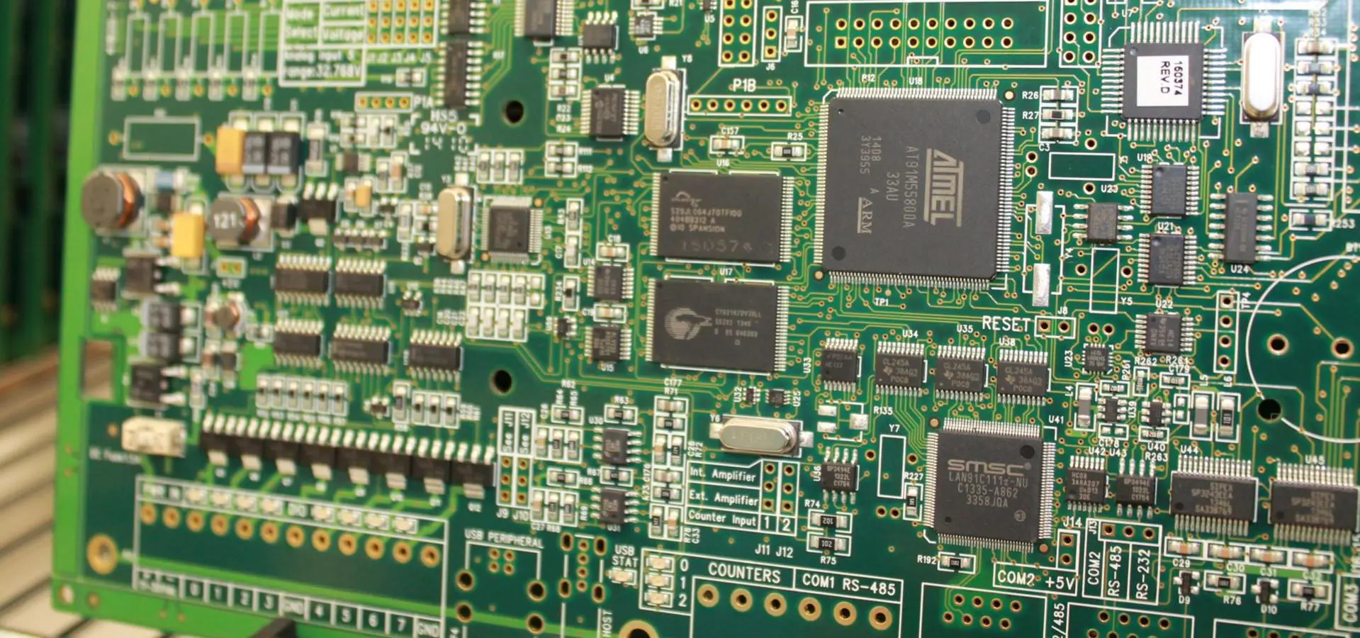
Tools and Materials Needed for Your DIY PCB Project
Before starting, gather the necessary tools and materials to ensure a smooth process. Here’s a detailed list tailored for a military communication PCB project:
- Copper-Clad Board: A single or double-sided board (1.6mm thickness is ideal for durability).
- Laser Printer: For printing your circuit design using the toner transfer method.
- Glossy Paper or Transfer Film: To transfer the design onto the copper board.
- Etchant Solution: Ferric chloride or a safer alternative like hydrogen peroxide and hydrochloric acid mix for etching the copper.
- Drill and Bits: A small hand drill or rotary tool with 0.8mm-1.2mm bits for component holes.
- Soldering Iron and Solder: A 25-40W iron with fine tip and lead-free solder for assembly.
- Components: Resistors, capacitors, transistors, or a simple IC for a basic transmitter/receiver circuit (e.g., operating at 433 MHz for short-range communication).
- Multimeter: For testing continuity and voltage after assembly.
- Safety Gear: Gloves, goggles, and a well-ventilated workspace for handling chemicals during etching.
Step 1: Designing Your Military Communication Circuit
The first step in any PCB project is designing the circuit. For a simple military communication application, consider building a low-power radio frequency (RF) transmitter or receiver. A basic design could operate at a frequency like 433 MHz, which is commonly used for short-range communication and is legal in many regions for unlicensed use at low power levels (typically under 10mW). Use free, open-source software to create your schematic and layout. Focus on a compact design with minimal components to keep it beginner-friendly, while ensuring traces are wide enough (at least 0.5mm) to handle potential power surges—a nod to military durability.
Keep signal integrity in mind by minimizing trace lengths for RF signals to reduce impedance mismatches. For example, at 433 MHz, the wavelength is approximately 69 cm, so keep critical traces under 10% of this length (about 6.9 cm) to avoid significant signal loss. Once your design is ready, print it on glossy paper or transfer film using a laser printer, ensuring the toner is dark and even for a clean transfer.
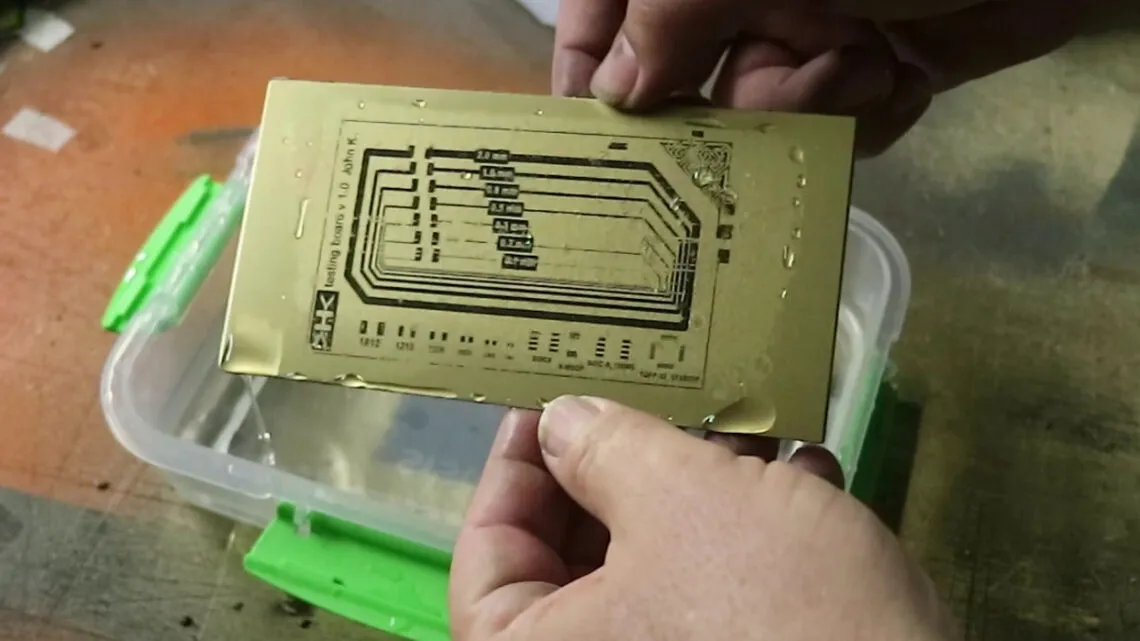
Step 2: Toner Transfer Method for PCB Layout
The toner transfer method is a popular DIY technique to transfer your circuit design onto a copper-clad board. Start by cleaning the copper surface with steel wool or sandpaper to remove oxidation, then wipe it with isopropyl alcohol for a spotless finish. Place the printed design face-down on the copper and secure it with tape. Use a household iron set to high heat (no steam) to press the design onto the board for 5-10 minutes, applying firm, even pressure. The heat melts the toner, bonding it to the copper.
After cooling, soak the board in water for 10-15 minutes to soften the paper, then gently peel or rub it off, leaving the toner pattern behind. Inspect the design for any breaks or smudges, and touch up with a permanent marker if needed. This step is crucial for ensuring your traces are precise, especially for RF circuits where even small errors can disrupt signal performance.
Step 3: Etching the PCB
Etching removes the unprotected copper, leaving only your circuit traces. Prepare your etchant solution in a plastic container—ferric chloride is a common choice, but a mix of hydrogen peroxide (3%) and hydrochloric acid (30%) in a 2:1 ratio works faster and is often safer with proper precautions. Wear gloves and goggles, and work in a ventilated area. Submerge the board in the solution, agitating it gently every few minutes. The process typically takes 10-30 minutes, depending on the solution strength and copper thickness.
Once the exposed copper is gone, remove the board, rinse it thoroughly with water, and clean off the toner with acetone or sandpaper. You’ll now have a board with clear copper traces ready for drilling. For military applications, double-check that traces are intact, as any discontinuity could compromise reliability in a real-world scenario.
Step 4: Drilling Holes for Components
Drilling is next, creating holes for component leads and mounting points. Use a small hand drill or rotary tool with bits sized between 0.8mm and 1.2mm, depending on your component leads. Mark hole locations with a center punch to prevent the drill from slipping. Drill slowly and steadily to avoid damaging the board or breaking bits. For a military-inspired design, consider adding extra mounting holes for securing the PCB in a protective enclosure, mimicking the rugged setups used in field equipment.
After drilling, clean the board with a brush to remove debris. Precision is key here—misaligned holes can make soldering difficult and affect the circuit’s performance. If you’re working with a double-sided board, ensure holes align perfectly on both sides for through-hole components.
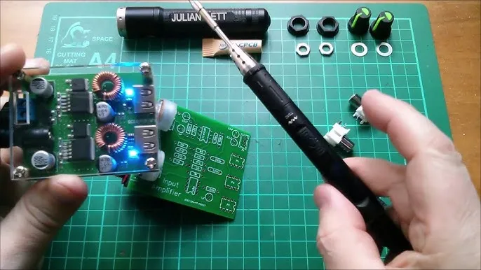
Step 5: Soldering Components onto the PCB
Soldering brings your PCB to life by attaching components to the board. Heat your soldering iron to around 300°C (572°F) for lead-free solder, and ensure the tip is clean. Start with smaller components like resistors and capacitors, placing them through the drilled holes and bending the leads slightly to hold them in place. Apply a small amount of solder to the iron tip, touch it to the pad and lead simultaneously, and feed solder into the joint until it forms a shiny, cone-shaped bond. Avoid overheating, as it can damage components or lift traces—critical for military designs where reliability is paramount.
For RF components, keep leads short to minimize interference. Once all components are soldered, trim excess leads with cutters and inspect for cold joints (dull, grainy connections) that could fail under stress. A well-soldered board ensures stable operation, even in simulated harsh conditions.
Step 6: Testing Your Military Communication PCB
Testing is crucial to verify that your PCB functions as intended. Use a multimeter to check for continuity between traces, ensuring there are no shorts or open circuits. Power up the board with a suitable voltage (e.g., 5V or 9V, depending on your design) and measure key points to confirm correct operation. For a communication circuit, test signal transmission or reception using a simple antenna and a receiver tuned to your frequency (e.g., 433 MHz). Check for a clear signal over a short range—10 to 20 meters is a reasonable goal for a basic DIY setup.
Simulate military-like conditions by exposing the board to minor stress, such as temperature variations (e.g., placing it in a fridge at 5°C for an hour, then testing again). While it won’t match true military testing (which might involve vibration at 10-2000 Hz), this gives insight into durability. If issues arise, troubleshoot by inspecting solder joints and component values.
Military Applications and Considerations for DIY PCBs
While a home-built PCB won’t meet full military standards, you can incorporate design principles inspired by military applications. Focus on durability by using thicker boards (1.6mm or more) and applying a protective coating like conformal coating to shield against moisture and dust—common in field environments. Design for low power consumption, as military devices often operate on limited battery life, targeting efficiency with components that draw minimal current (e.g., under 50mA in standby mode).
Consider secure communication by avoiding easily intercepted frequencies or adding basic encryption if your skills allow. Remember that military communication often prioritizes reliability over complexity, so keep your design simple yet robust. This project can serve as a stepping stone to understanding real-world applications like field radios or emergency beacons, even if it’s just for learning purposes.
Tips for Success in Your DIY PCB Project
To ensure your military communication PCB project succeeds, follow these additional tips:
- Double-Check Your Design: Before printing or etching, verify your layout for errors using simulation tools if possible.
- Work Safely: Handle chemicals and soldering equipment with care to avoid injury or damage.
- Start Simple: If you’re new to RF circuits, begin with a basic transmitter before tackling complex designs.
- Document Everything: Keep notes on your process to troubleshoot or replicate the project later.
- Test Incrementally: Assemble and test in stages to catch issues early.
Conclusion: Mastering DIY PCB for Military Communication
Building a simple military communication PCB at home is a rewarding challenge that sharpens your skills in DIY PCB techniques like etching, toner transfer, drilling, soldering, and testing. By following this step-by-step guide, you’ve learned how to design a basic communication circuit, transfer and etch the layout, assemble components, and test for functionality with military-inspired durability in mind. While this project is a simplified version of true military hardware, it provides valuable insights into the principles of rugged electronics design.
Whether you’re experimenting for fun or preparing for more advanced projects, the skills gained here—combined with a focus on reliability and efficiency—can be applied to countless other endeavors. Take pride in your creation, and continue exploring the fascinating world of electronics with confidence. For high-quality PCB materials and support, trust us at ALLPCB to provide the resources you need to bring your ideas to life.


