 ALLPCB


In the world of electronics, high speed PCB design is a critical skill for creating circuits that handle fast signals without losing data or performance. Whether you're working on aerospace PCB design, defense PCB design, signal integrity PCB projects, or metal core PCB applications, mastering high speed design ensures reliability and efficiency. At ALLPCB, we’re here to guide you through the essentials of high speed PCB design, offering practical tips and insights tailored to these specialized fields.
In this comprehensive guide, we’ll explore what high speed PCB design entails, why it’s crucial for industries like aerospace and defense, and how to address challenges like signal integrity and thermal management with metal core PCBs. Let’s dive into the details to help you build robust, high-performing circuits.
What Is High Speed PCB Design?
High speed PCB design refers to the process of creating printed circuit boards that can handle signals with very fast rise and fall times, often in the range of gigahertz (GHz) frequencies. These designs are essential for modern electronics where data transfer rates exceed 100 MHz, such as in telecommunications, computing, and advanced military systems. The primary goal is to maintain signal integrity, minimize noise, and ensure the circuit operates reliably under demanding conditions.
In fields like aerospace PCB design and defense PCB design, high speed circuits are used in radar systems, avionics, and communication devices where even a small signal delay or distortion can lead to critical failures. For instance, a radar system in a defense application might operate at frequencies above 1 GHz, requiring precise trace layouts to prevent signal reflection or crosstalk.
Why High Speed PCB Design Matters in Aerospace and Defense
Industries like aerospace and defense have unique demands for PCBs due to extreme environments and the need for absolute reliability. High speed PCB design plays a vital role in meeting these requirements.
Aerospace PCB Design: Precision in Harsh Conditions
In aerospace PCB design, circuits must withstand high altitudes, temperature swings from -55°C to 125°C, and intense vibrations. High speed designs are used in flight control systems, navigation equipment, and satellite communications, where signals must travel without interference at speeds exceeding 500 MHz. A key challenge is ensuring that the dielectric materials used in the PCB can maintain consistent performance under these conditions. Materials with low dielectric constants (Dk), such as PTFE-based laminates, are often chosen to minimize signal delay.
For example, a satellite communication system might require a PCB to process signals at 2.4 GHz. If the traces are not designed with proper impedance matching (typically targeting 50 ohms for RF signals), signal reflections can occur, leading to data loss or system failure.
Defense PCB Design: Security and Reliability
Defense PCB design focuses on ruggedness and security alongside high speed performance. Military applications like missile guidance systems or encrypted communication devices rely on PCBs that can handle multi-gigabit data rates while resisting electromagnetic interference (EMI). High speed design in this context often involves multilayer boards with dedicated ground planes to shield sensitive signals from external noise.
In a typical defense radar system, signal frequencies can reach up to 10 GHz. Designers must carefully plan trace widths and spacing to control impedance and reduce crosstalk, ensuring the system detects targets accurately even in hostile environments.
Signal Integrity in High Speed PCB Design
Signal integrity is at the heart of high speed PCB design. It refers to the ability of a signal to maintain its quality as it travels through the circuit, without distortion, delay, or interference. For signal integrity PCB projects, engineers must address several challenges to ensure optimal performance.
Common Signal Integrity Challenges
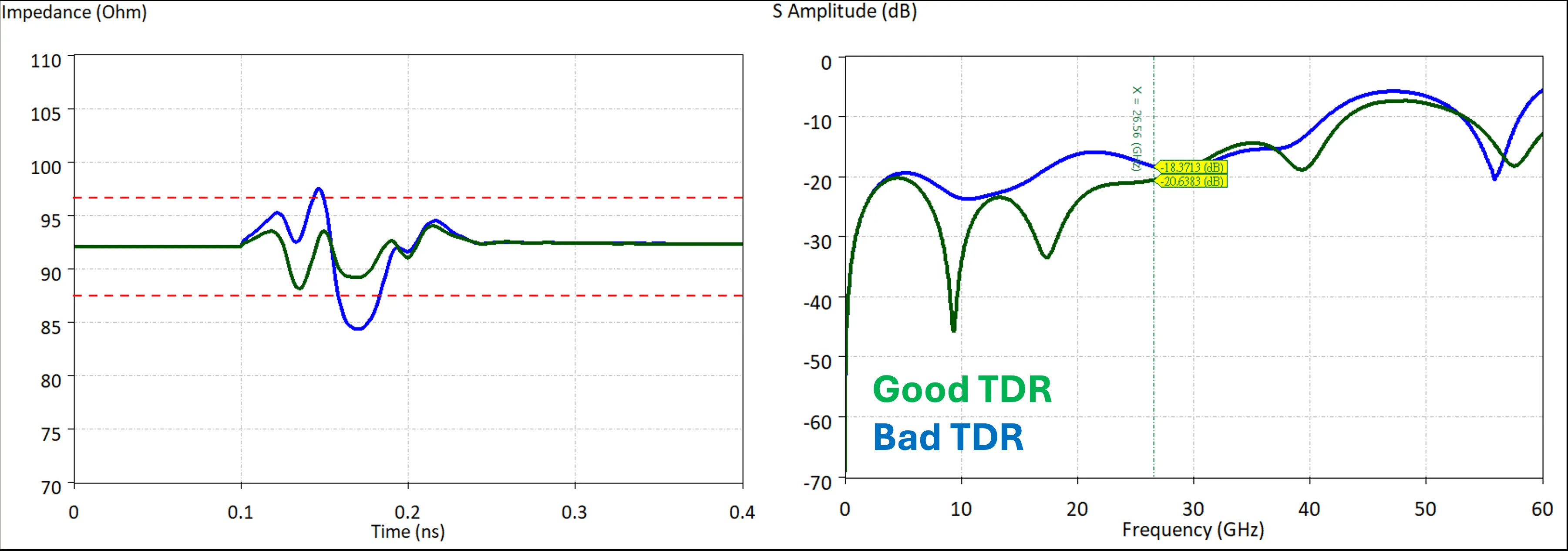
1. Signal Reflection: Occurs when there’s a mismatch in impedance along the signal path. For instance, if a trace designed for 50 ohms encounters a connector with 75 ohms impedance, part of the signal bounces back, causing errors. This is common in high speed designs operating above 1 GHz.
2. Crosstalk: Happens when signals on adjacent traces interfere with each other. At frequencies above 500 MHz, traces spaced less than 10 mils apart can induce unwanted noise, especially in densely packed boards.
3. Timing Errors: In high speed systems, even a delay of 100 picoseconds can misalign data, leading to system crashes. This is critical in applications like DDR memory interfaces, where timing precision is non-negotiable.
4. Electromagnetic Interference (EMI): High speed signals can radiate energy, interfering with nearby circuits. Proper grounding and shielding are essential to minimize EMI, especially in defense and aerospace PCB design.
Solutions for Signal Integrity
To maintain signal integrity, designers use several techniques:
- Impedance Matching: Calculate trace widths and dielectric thickness to achieve a target impedance, often 50 or 100 ohms, using tools like field solvers.
- Proper Routing: Route high speed traces as straight as possible, avoiding sharp corners that can cause signal reflection. Use differential pairs for signals like USB or PCIe, maintaining equal lengths within 5 mils for paired traces.
- Ground Planes: Place continuous ground planes beneath signal layers to provide a return path and reduce EMI. Split ground planes should be avoided unless necessary for analog-digital separation.
- Decoupling Capacitors: Position capacitors (e.g., 0.1 μF) near power pins of ICs to stabilize voltage and filter noise in high speed circuits.
Metal Core PCB in High Speed Design: Managing Heat
High speed circuits often generate significant heat due to fast switching and high power components. This is where metal core PCB technology becomes invaluable, especially in aerospace and defense applications where thermal management is critical.
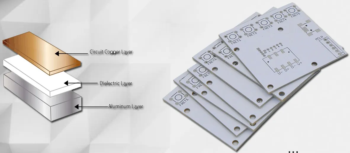
What Is a Metal Core PCB?
A metal core PCB uses a metal base layer, typically aluminum or copper, instead of the standard FR-4 fiberglass. This metal layer acts as a heat sink, dissipating heat away from components and preventing thermal buildup. In high speed designs, where components like processors or RF amplifiers can reach temperatures above 100°C, a metal core PCB ensures longevity and reliability.
Benefits for High Speed Applications
- Thermal Dissipation: Metal core PCBs can handle power densities up to 10 W/cm2, making them ideal for high speed systems with intense heat output.
- Durability: The metal base adds mechanical strength, which is crucial for aerospace PCB design where boards face vibration and shock.
- Signal Stability: By keeping components cool, metal core PCBs help maintain consistent electrical performance, reducing signal drift caused by temperature changes.
For example, in a defense communication system with high speed RF signals at 5 GHz, a metal core PCB can prevent overheating of power amplifiers, ensuring the system operates without interruption even under continuous use.
Key Guidelines for High Speed PCB Design
Creating a successful high speed PCB requires following best practices tailored to your specific application, whether it’s aerospace PCB design, defense PCB design, or signal integrity PCB projects. Here are actionable tips to guide your process:
1. Choose the Right Materials
Select PCB materials with low dielectric loss for high frequency signals. For instance, Rogers RO4003C has a dielectric constant of 3.38 and low loss tangent, making it suitable for frequencies up to 10 GHz. In contrast, standard FR-4 may only be reliable up to 1 GHz due to higher signal loss.
2. Optimize Stack-Up Design
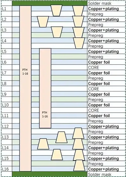
Plan your PCB stack-up to alternate signal and ground layers. A typical 6-layer high speed PCB might follow a signal-ground-signal-power-ground-signal configuration to minimize noise. Keep high speed signals on outer layers for easier routing and impedance control.
3. Control Trace Lengths
For high speed signals, keep trace lengths as short as possible to reduce delay. In differential pairs, match lengths within 1-2 mils to prevent skew. Use simulation tools to verify timing before manufacturing.
4. Minimize Vias
Vias introduce inductance and capacitance, disrupting high speed signals. If unavoidable, use back-drilling to remove unused via stubs, especially for signals above 2 GHz.
5. Test and Simulate
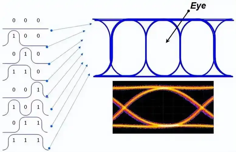
Before production, use simulation software to model signal behavior and identify potential issues like crosstalk or reflection. Post-manufacturing, perform tests with oscilloscopes to measure rise times and eye diagrams for data integrity.
Challenges and Future Trends in High Speed PCB Design
As technology advances, high speed PCB design faces new challenges and opportunities, especially in aerospace and defense sectors.
Current Challenges
- Higher Frequencies: With 5G and beyond pushing frequencies to 28 GHz and higher, maintaining signal integrity becomes increasingly complex.
- Miniaturization: Devices are shrinking, forcing designers to pack high speed traces into smaller spaces without sacrificing performance.
- Environmental Extremes: Aerospace PCB design must account for radiation in space, while defense PCB design needs to resist chemical exposure and humidity.
Emerging Trends
- Advanced Materials: New laminates with ultra-low dielectric constants are being developed to support frequencies above 50 GHz.
- AI in Design: Artificial intelligence is being integrated into design tools to optimize trace routing and predict signal integrity issues before fabrication.
- Flexible High Speed PCBs: Flexible and rigid-flex designs are gaining traction in aerospace for lightweight, compact systems with high speed capabilities.
Conclusion: Mastering High Speed PCB Design with ALLPCB
High speed PCB design is a cornerstone of modern electronics, especially in demanding fields like aerospace PCB design and defense PCB design. By focusing on signal integrity PCB techniques and leveraging technologies like metal core PCB for thermal management, engineers can build circuits that meet the toughest performance standards. At ALLPCB, we’re committed to supporting your high speed design journey with top-quality manufacturing and expert guidance.
Whether you’re designing for a satellite communication system, a military radar, or a high speed data interface, following the guidelines and insights in this blog can help you achieve reliable, efficient results. Start applying these principles today to elevate your PCB projects to new heights.


