ALLPCB


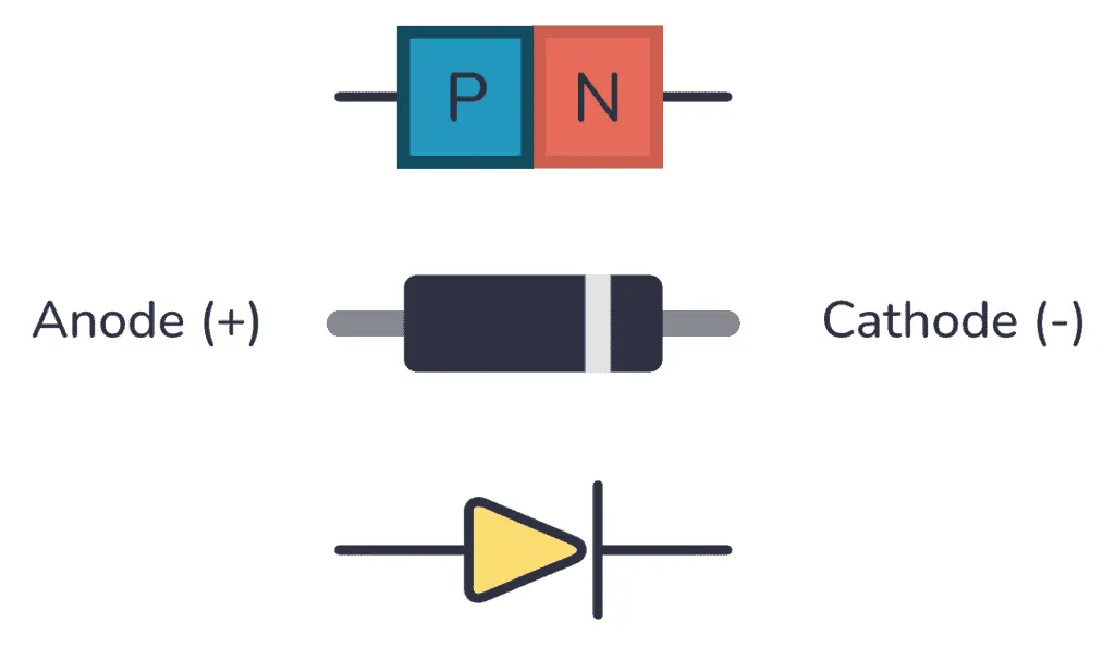
Diodes are semiconductor devices formed by a PN junction. When the applied voltage exceeds the junction threshold, current flows through the diode; under reverse bias the diode remains nonconductive as long as the voltage does not exceed the breakdown level. In the nonconductive state the reverse-biased PN junction prevents electron flow, so the diode behaves like an open circuit.
A clamping diode uses these conduction and nonconduction characteristics to manipulate an input voltage. A clamping circuit fixes part of an input or output signal waveform to a chosen reference level. In other words, it clamps the waveform to a specified DC level.
What Is a Diode Clamping Circuit?
A diode clamping circuit positions either the positive or negative peaks of a signal at a desired DC level. A DC offset is simply added to or subtracted from the input signal. Clamping circuits are also called IC restorers or AC signal level converters.
In some systems, for example video receivers, a signal can lose its DC component when passing through a coupling capacitor network. A clamping circuit is used to restore a DC level to the signal input. Although the restored DC level may not match the original lost DC component exactly, the clamping ensures that the waveform peaks are referenced to a defined level.
How the Diode Clamp Circuit Works
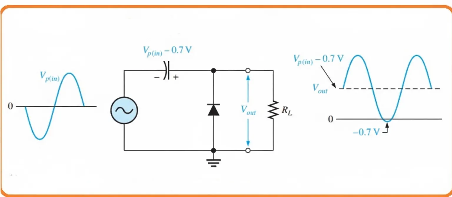
Assume the negative half-cycle charges the capacitor through the diode. During the negative half of the input, the signal diode is forward biased and the capacitor charges to approximately Vp(in) minus the diode forward drop (about 0.7 V). After the negative peak the diode becomes reverse biased because the cathode sits near the capacitor charge value Vp(in) - 0.7 V. The capacitor discharges through the load resistor R_L, so the charge change from one negative half-cycle to the next is small and depends on R_L.
If the capacitor loses charge during the input signal, the clamping action will be disturbed. For efficient clamping, the RC time constant should be much larger than the input period. If the time constant RC is about 100 times the input period, clamping efficiency is high. If RC is about 10 times the input period, the baseline shift at ground will still be small due to charging currents.
The capacitor will hold a charge approximately equal to the input signal peak minus the diode drop. The capacitor's voltage acts like a battery in series with the input signal, adding a DC component to the input. The output is the superposition of the input AC and the capacitor-derived DC offset, as shown below.
Positive and Negative Clamps
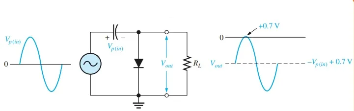
By changing the diode position, a negative DC offset can be added to the input signal to produce a negative clamp output. This arrangement is called a negative clamp.
Practical Components and Design Guidelines
A basic clamp circuit requires at least three components: a diode, a capacitor, and a resistor. Sometimes an external DC supply is added to shift the clamped level. Key points:
- The waveform shape remains the same, only its DC level shifts up or down.
- The peak-to-peak or RMS amplitude does not change, so input and clamped output have the same peak-to-peak value, 2Vmax. AC voltmeters will read the same for input and clamped output.
- Values of R and C affect waveform fidelity.
- Choose R and C so that the time constant t = RC is large enough that the capacitor voltage does not change significantly during diode nonconducting intervals. A good rule is t = RC at least 10 times the input period.
Clamping Circuit Types
Positive Clamping
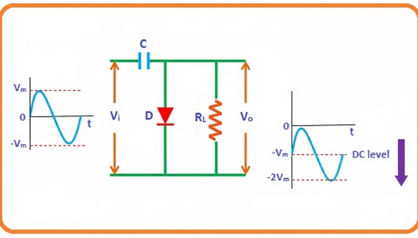
The positive clamping circuit consists of the input source Vi, capacitor C, diode, and load resistor. During the negative half-cycle the diode is forward biased and charges C to the input peak Vm with a polarity opposite to the signal across the diode. After the negative peak the diode is reverse biased and the capacitor holds its charge. During the positive half-cycle the diode is reverse biased and no current flows through it, so the capacitor voltage adds to the input source across the load and the output shifts upward. The output amplitude becomes the sum of the input peak and the capacitor voltage, effectively shifting the signal upward.
Negative Clamping
In the negative clamp, during the positive input half-cycle the diode is forward biased and charges the capacitor to the negative of the input peak -Vm. During the negative half-cycle the diode is reverse biased and the capacitor voltage combines with the input to shift the waveform downward, producing an output that is offset below the original baseline.
Bias Clamping
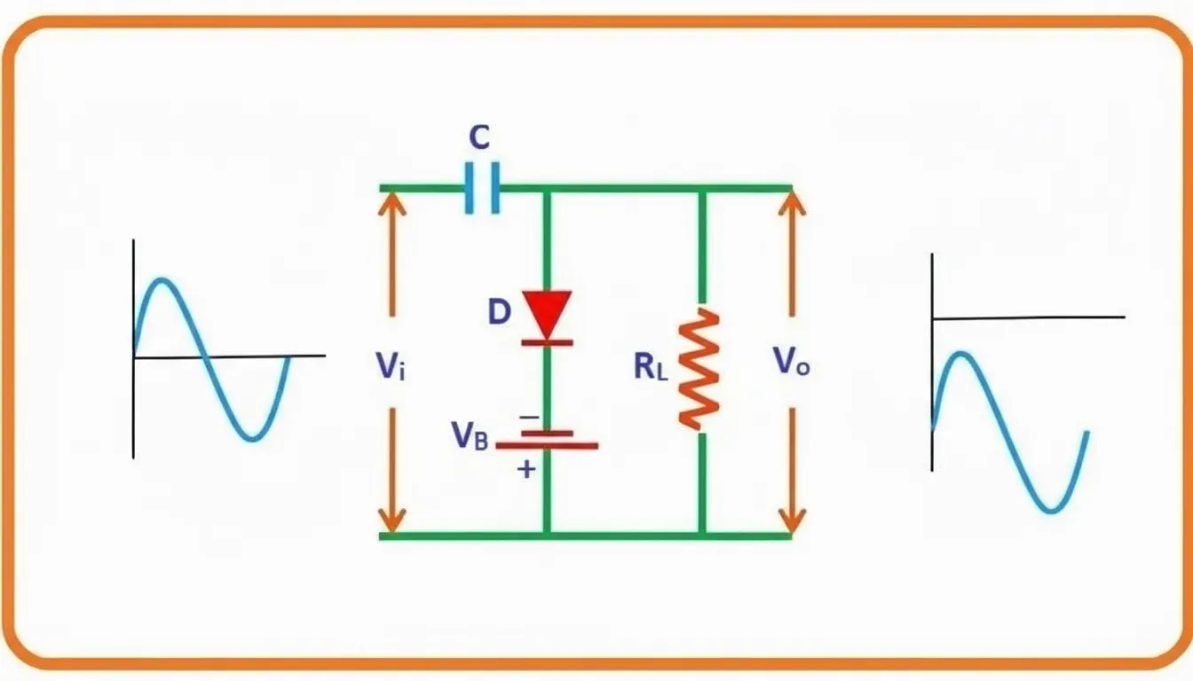
When an additional DC offset is required, a bias clamping circuit is used. The difference from an unbiased clamp is that a DC source provides an extra offset.
Positive Bias with Positive Clamp
With a positive DC supply connected as shown, the DC source can forward bias the diode during certain input intervals and charge the capacitor accordingly. When the input exceeds the DC source voltage the diode becomes reverse biased and stops conducting.
Negative Bias with Positive Clamp
With a negative DC bias, the diode conduction depends on the relative magnitudes of the input and battery voltages. If the battery voltage is greater than the input, the diode remains reverse biased; if the input exceeds the battery, the diode conducts and charges the capacitor.
Positive Bias with Negative Clamp
With positive bias applied to a negative clamp, diode conduction and capacitor charging depend on the relative voltages of the input and the bias source. During intervals where the diode is reverse biased, the signal appears across the load resistor and the combined voltages determine the output amplitude.
Negative Bias with Negative Clamp
When the bias and input polarities change, conduction states flip accordingly and the output follows the sum of input and capacitor voltages or the bias-limited levels.
Clamping Diode Protection Circuits
Clamping protection can be implemented with two diodes connected anti-series. Only one diode conducts at a time, so the clamped voltage is limited to the diode forward drop in either direction, typically about 0.5 to 0.7 V. The clamp protects downstream circuitry by preventing excessive voltage across protected nodes.
Consider a rectangular input waveform clamped so that the top is held near a reference level. When the diode conducts, the capacitor rapidly charges to the input amplitude and the output steps accordingly. When the diode is off the capacitor discharges slowly through R, so the output changes little between conduction intervals. Repeating this cycle limits the waveform top to the reference level, hence a top or positive peak clamping circuit. Reversing the diode orientation clamps the waveform bottom, producing a negative peak clamp.
Transistor base-emitter junctions can also act as clamps if treated as diodes; the same clamping principle applies but with amplification provided by the transistor.
Choosing Component Values
Clamping performance is governed by the capacitor time constant. Select R and C so the time constant prevents significant discharge during diode nonconducting intervals. To avoid rapid capacitor discharge, use a large resistance and a relatively small capacitance so charging during conduction intervals remains fast.

Applications of Diode Clamps
- Transient protection: Clamping diodes provide useful protection against transient events such as ESD and surge. When the input exceeds a threshold, a diode conducts and redirects excess current away from the load. A series resistor is often placed before the diode to limit current and keep the diode within safe operating range.
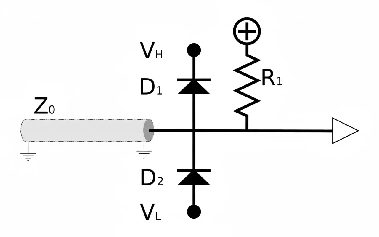
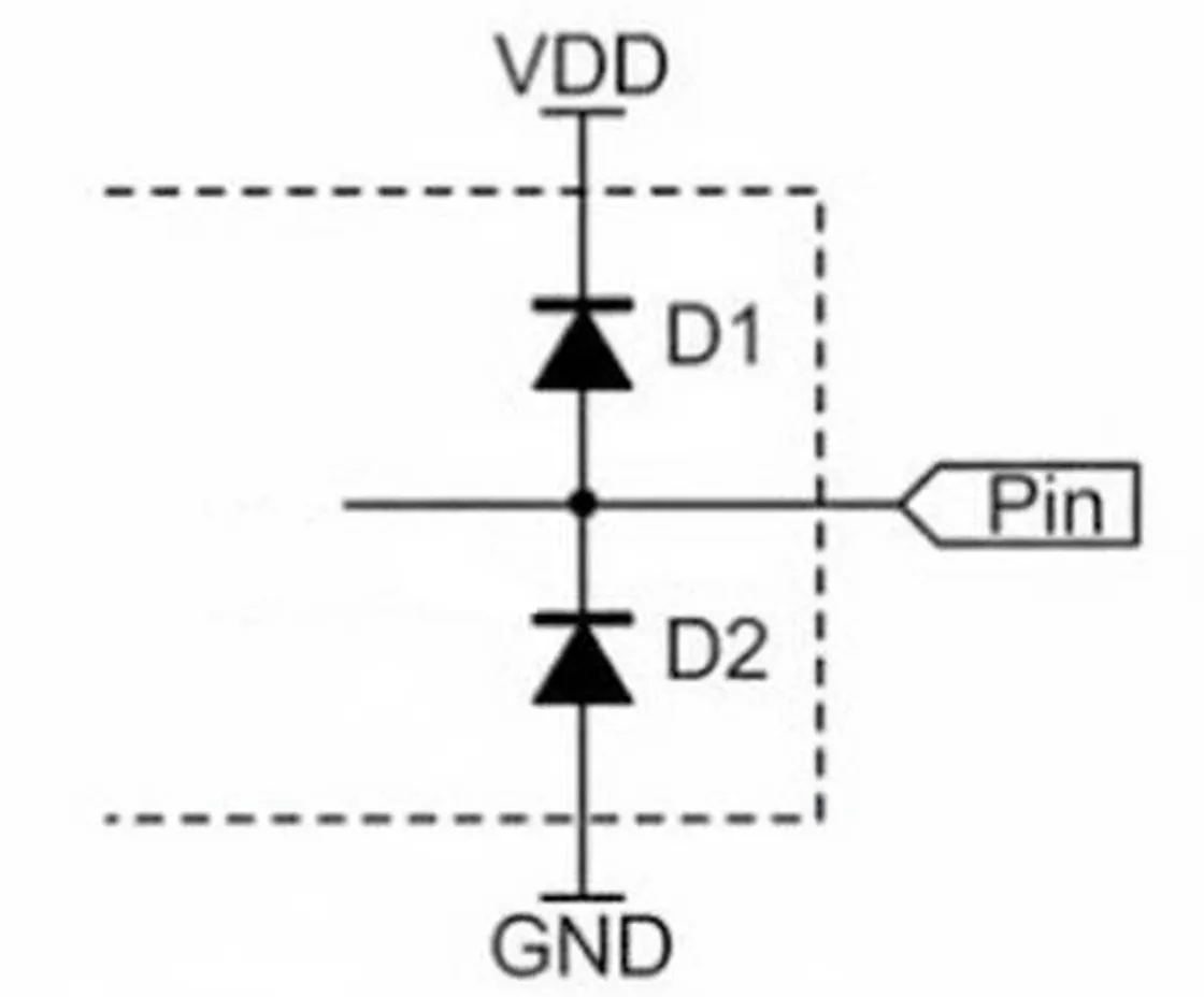
- GPIO protection: Internal clamping diodes are commonly used on microcontroller I/O pins to prevent voltages outside the supply range from damaging internal circuits. A typical internal structure clamps input voltages that go above VCC or below ground.
Related Reading: What Is GPIO? Architecture and Working Principle
- Other uses: Clamping circuits restore DC components in display systems such as oscilloscopes and radar displays to prevent image displacement caused by scanning speed changes. In television systems, clamps hold the tops of synchronization pulses at a fixed voltage to enable reliable separation of sync and video despite DC loss or interference.
- Clamping diodes generate a clamp voltage used to protect components that require overvoltage limiting, for example protecting a MOSFET in a switching power supply by limiting the voltage between drain and source.
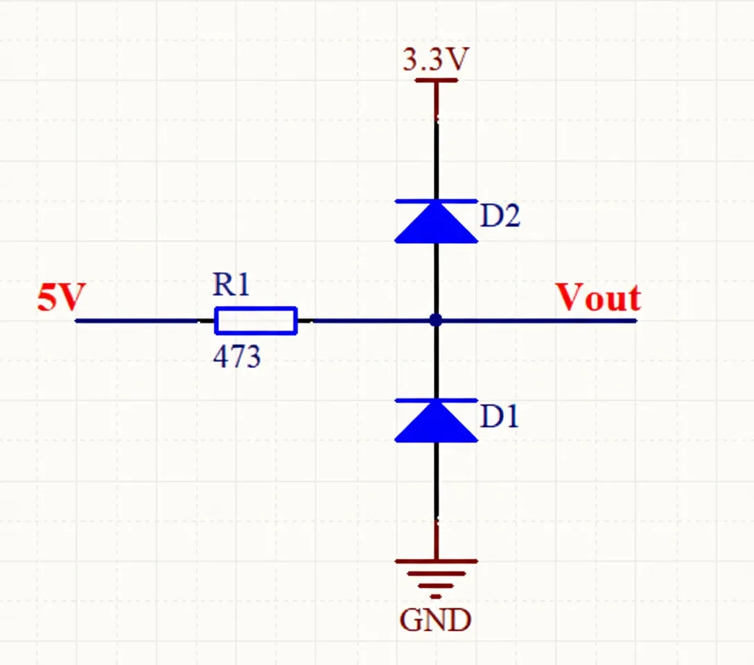
Example: Simple Clamp Protection for an Input Node
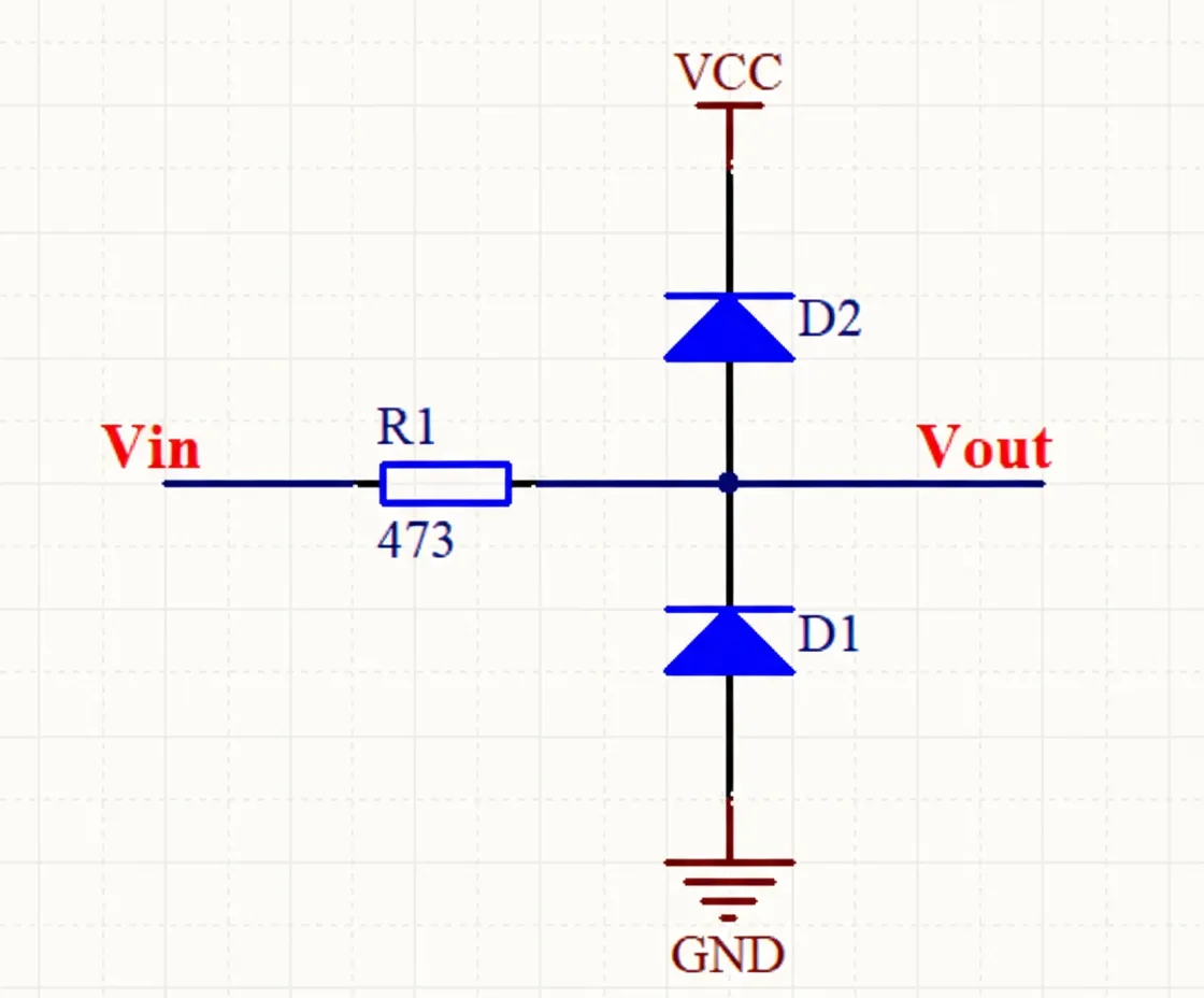
This clamp protection circuit keeps the input node voltage Vout clamped between VCC and ground. The operation is:
- If Vin is greater than VCC, D2 conducts and D1 is off, so Vout is limited to approximately VCC plus one diode drop.
- If Vin is between VCC and ground, both diodes are off and Vout equals Vin.
- If Vin is less than ground, D1 conducts and D2 is off, so Vout is limited to approximately ground minus one diode drop.
Thus, regardless of Vin, Vout stays within the range set by the clamp and protects downstream circuitry from overvoltage.
Related Reading: Working Principle of Diode Protection Circuits
Typical Application Scenarios
- Microcontroller I/O protection: When an external analog signal is applied to an MCU pin, a diode clamp can prevent overvoltage from damaging the internal circuits. If the MCU already integrates protection diodes, an external clamp may be unnecessary.
- Level shifting: When interfacing systems with different logic levels, for example 5 V and 3.3 V domains, a simple diode clamp can limit a 5 V signal to safe levels for a 3.3 V device without adding an active level-shifter IC.
The above covers diode clamp protection circuit applications and basic design considerations.