 ALLPCB


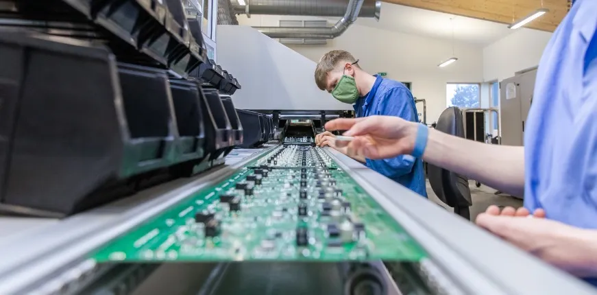
Wave soldering is a critical process in mass production of printed circuit boards (PCBs), especially for through-hole components. If you're looking to optimize your manufacturing process, achieve high yields, and minimize defects, understanding wave soldering process control in mass production is essential. This blog dives deep into key strategies like maintaining a wave soldering machine maintenance schedule, minimizing solder bridging in wave soldering, optimizing wave height for solder quality, and mastering wave soldering temperature control. Let’s explore how to perfect this process for consistent, high-quality results in large-scale production.
What Is Wave Soldering and Why It Matters in Mass Production
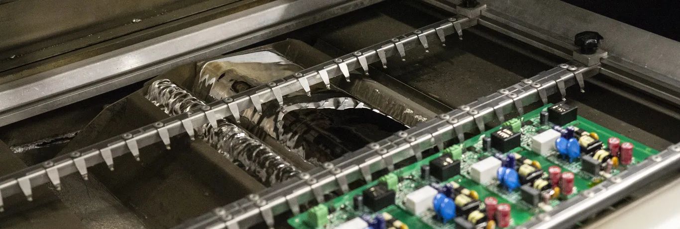
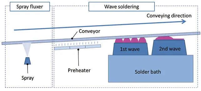
Wave soldering is a bulk soldering technique used to attach electronic components to PCBs. In this process, a PCB passes over a molten solder wave, which creates reliable mechanical and electrical connections between through-hole components and the board. This method is ideal for mass production because it’s fast, efficient, and can handle large volumes of assemblies with consistent results.
In mass production, wave soldering stands out for its ability to reduce manual labor and ensure uniformity. However, achieving high yields—meaning a high percentage of defect-free boards—requires precise control over every aspect of the process. Defects like solder bridging, insufficient wetting, or thermal stress can lead to costly rework or product failures. That’s why mastering wave soldering process control in mass production is a top priority for manufacturers aiming for efficiency and quality.
Key Steps in the Wave Soldering Process for Mass Production
The wave soldering process involves several stages, each of which must be carefully managed to ensure high yields. Here’s a breakdown of the key steps:
- Flux Application: A flux layer is applied to clean the metal surfaces on the PCB and components, ensuring proper solder adhesion.
- Preheating: The board is preheated to activate the flux and prevent thermal shock when it contacts the molten solder. Typical preheat temperatures range from 100°C to 150°C, depending on the board material and components.
- Solder Wave Contact: The PCB passes over a wave of molten solder, usually at a temperature of 250°C to 260°C for lead-free solder, which bonds the components to the board.
- Cooling: The board cools down to solidify the solder joints, completing the process.
Each of these steps must be optimized for mass production to avoid defects and ensure consistent quality across thousands of boards.
Wave Soldering Process Control in Mass Production
Controlling the wave soldering process in mass production is the foundation of achieving high yields. Without strict oversight, variations in temperature, wave height, or conveyor speed can lead to defects. Here are key control points to focus on:
1. Conveyor Speed Consistency
The speed at which the PCB moves over the solder wave directly impacts solder joint quality. A speed of 1.0 to 1.5 meters per minute is often ideal for most setups, though this can vary based on board design and component density. Too fast, and the solder may not wet properly; too slow, and excess solder can cause bridging.
2. Flux Application Uniformity
Flux must be applied evenly to prevent areas of poor wetting. Use automated fluxers with regular calibration to ensure consistent coverage. Check flux density weekly, aiming for a specific gravity of around 0.80 to 0.85 for alcohol-based fluxes.
3. Monitoring Solder Bath Composition
The solder bath can become contaminated with impurities like copper or iron over time, affecting joint quality. Regularly test the solder composition—ideally every 1,000 boards or weekly in high-volume production—and replenish or replace the solder to maintain a tin content of at least 63% for traditional Sn63Pb37 alloy or as per manufacturer specs for lead-free solder.
By maintaining tight control over these variables, manufacturers can significantly reduce defect rates in mass production environments.
Wave Soldering Machine Maintenance Schedule for Peak Performance
A well-maintained wave soldering machine is crucial for minimizing downtime and ensuring consistent results. Neglecting maintenance can lead to uneven wave height, temperature fluctuations, or flux buildup, all of which cause defects. Here’s a recommended wave soldering machine maintenance schedule for mass production setups:
- Daily: Clean flux residues from the machine’s conveyor and fluxer nozzles to prevent buildup. Inspect the solder wave for dross (oxide layer) and skim it off to maintain a clean solder surface.
- Weekly: Check and calibrate temperature sensors to ensure the solder bath remains within ±5°C of the target (e.g., 250°C for lead-free solder). Inspect pump mechanisms for wear and ensure wave height stability.
- Monthly: Drain and replace the solder bath if contamination levels exceed 0.1% copper by weight. Lubricate moving parts like conveyor belts and check for alignment issues.
- Quarterly: Conduct a full machine overhaul, replacing worn components like heaters or seals, and verify that preheat zones are functioning within specified ranges (100°C to 150°C).
Sticking to this maintenance schedule helps prevent unexpected failures and ensures the machine operates at peak efficiency, supporting high yields in mass production.
Minimizing Solder Bridging in Wave Soldering
Solder bridging, where excess solder creates unintended connections between adjacent pins or pads, is a common defect in wave soldering. In mass production, even a 1% defect rate due to bridging can result in thousands of failed boards. Here are proven strategies for minimizing solder bridging in wave soldering:
1. Optimize PCB Design
Ensure adequate spacing between through-hole pins, ideally at least 2.54 mm (0.1 inch), to reduce the risk of solder connecting adjacent points. Use solder masks to protect areas where solder isn’t needed.
2. Adjust Wave Height and Angle
A wave height that’s too high can deposit excess solder, leading to bridging. Aim for a wave height where the PCB bottom is just immersed by 1-2 mm into the solder wave. Additionally, adjust the wave angle (often around 7 degrees) to ensure smooth solder flow without pooling.
3. Control Conveyor Speed and Direction
Experiment with conveyor speeds within the 1.0 to 1.5 meters per minute range to find the sweet spot for your specific board layout. Also, ensure the PCB travels in a direction that minimizes solder drag across closely spaced pins—often perpendicular to the pin rows.
By fine-tuning these factors, manufacturers can drastically cut down on solder bridging, improving overall yield rates.
Optimizing Wave Height for Solder Quality
Wave height is a critical parameter in achieving high-quality solder joints. If the wave is too low, solder may not reach all component leads, causing insufficient wetting. If it’s too high, excess solder can lead to bridging or icicles. Here’s how to approach optimizing wave height for solder quality:
1. Measure and Adjust Wave Height
Use a wave height gauge to ensure the solder wave contacts the PCB bottom by 1-2 mm. Most modern machines allow for precise adjustments via pump speed controls. Test with a sample board to confirm uniform solder coverage without overflow.
2. Monitor Wave Stability
An unstable wave, caused by pump issues or dross buildup, can create uneven solder joints. Check the wave profile daily and clean the solder bath to maintain a smooth, consistent wave shape.
3. Match Wave Height to Board Thickness
For thicker boards (e.g., 2.0 mm or more), a slightly higher wave may be needed to ensure solder penetration. For standard 1.6 mm boards, a lower wave height often suffices. Adjust based on trial runs and visual inspection of solder joints.
Optimizing wave height directly impacts solder quality, reducing defects and ensuring reliable connections in mass production.
Wave Soldering Temperature Control for High Yields
Temperature control is one of the most important factors in wave soldering. Incorrect temperatures can cause thermal stress, poor wetting, or component damage, all of which lower yields. Here are key techniques for wave soldering temperature control:
1. Maintain Solder Bath Temperature
For lead-free solder, keep the bath at 250°C to 260°C, with a tolerance of ±5°C. For traditional tin-lead solder, 240°C to 250°C is often sufficient. Use high-precision thermocouples to monitor and maintain this range continuously.
2. Optimize Preheat Temperature
Preheat the PCB to 100°C to 150°C before it reaches the solder wave. This minimizes thermal shock, which can crack components or warp boards. Adjust based on board material—FR-4 boards typically need around 120°C, while high-Tg materials may require slightly higher preheat.
3. Avoid Overheating Components
Ensure the contact time with the solder wave is short—typically 2 to 4 seconds—to prevent overheating sensitive components. Monitor component datasheets for maximum temperature tolerances (often around 260°C for 10 seconds for many ICs) and adjust process parameters accordingly.
Precise wave soldering temperature control minimizes defects like cold joints or thermal damage, ensuring high yields in mass production runs.
Common Challenges in Wave Soldering and How to Overcome Them
Even with strict process control, challenges can arise in wave soldering. Here are some common issues in mass production and solutions to address them:
- Insufficient Wetting: Caused by inadequate flux or low preheat temperatures. Increase flux coverage and ensure preheat is at least 100°C.
- Solder Balling: Often due to excess moisture or flux residue. Use a proper drying step before soldering and clean boards thoroughly.
- Thermal Stress: Minimize by optimizing preheat and keeping solder contact time under 4 seconds.
Addressing these challenges proactively keeps defect rates low and maintains production efficiency.
Benefits of Mastering Wave Soldering in Mass Production
When wave soldering is optimized, the benefits for mass production are clear:
- Higher Yields: Defect rates can drop below 0.5%, meaning more usable boards per run.
- Faster Production: Automated wave soldering can process hundreds of boards per hour, far outpacing manual methods.
- Cost Savings: Fewer defects mean less rework, saving time and materials in large-scale operations.
By focusing on process control, maintenance, and parameter optimization, manufacturers can unlock these advantages consistently.
Conclusion: Achieving Excellence in Wave Soldering
Wave soldering is a powerful tool for mass production of PCBs, but it demands precision to achieve high yields and minimize defects. By implementing strict wave soldering process control in mass production, adhering to a wave soldering machine maintenance schedule, minimizing solder bridging in wave soldering, optimizing wave height for solder quality, and mastering wave soldering temperature control, manufacturers can ensure reliable, high-quality results. These strategies not only improve efficiency but also reduce costs, making wave soldering a cornerstone of successful PCB assembly.
With the right approach, your production line can deliver consistent, defect-free boards, meeting the demands of today’s fast-paced electronics industry. Focus on the details, monitor your process, and maintain your equipment to stay ahead in the game.


