ALLPCB


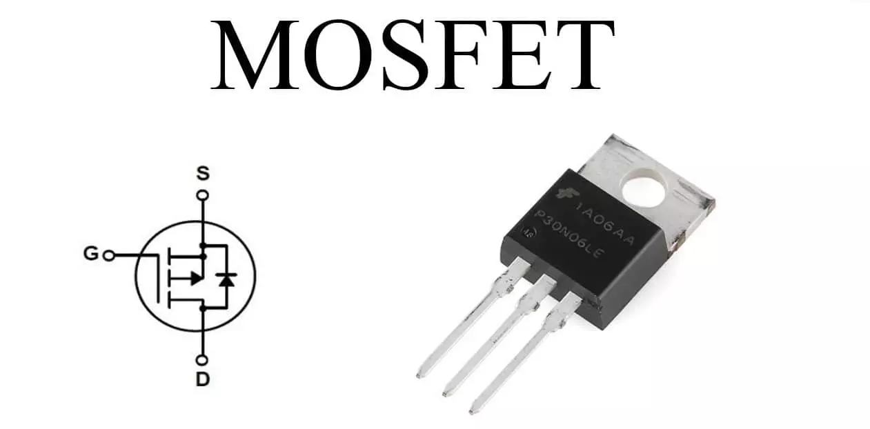
Key Ratings
VDSS: Maximum drain-to-source voltage; must not exceed -60 V.
VGSS: Maximum gate-to-source voltage that can be tolerated, ±20 V.
ID: Maximum continuous drain current, -130 mA.
IDM: Pulse peak current. Power MOSFETs generally have higher peak current capability for PWM switching.
PD: Maximum device power dissipation, 225 mW at 25°C. Derate above 25°C; for each 1°C rise, reduce by 1.8 mW.
RθJA: Thermal resistance from junction to ambient, 556 °C/W.
Tj: Maximum junction temperature and maximum storage temperature, 150 °C.
TL: Maximum temperature the package can withstand briefly during soldering processes such as manual soldering, reflow, or wave soldering.
Related Reading: Understanding MOSFET Datasheet Parameters
Thermal Parameters and Calculation
Junction temperature and thermal resistance are used to determine junction heating. If the junction temperature rises above the maximum, device damage can occur. Calculate as follows:
Tj = Ta + (RθJA × PD)
Ta = ambient temperature around the package (°C)
RθJA = thermal resistance from the P-N junction to ambient (°C/W) (provided in datasheets)
PD = package power dissipation (W). Chip power dissipation = Pin - Pout
Ways to Reduce Junction Temperature
- Reduce the device intrinsic thermal resistance;
- Provide effective secondary heat sinking;
- Reduce thermal resistance at the interface between the device and the secondary heat sink;
- Limit the applied power;
- Lower the ambient temperature.
Leakage and Breakdown
VBRDSS: Drain-to-source breakdown voltage at VGS = 0.
IDSS: Drain current at zero gate voltage, measured with VGS = 0 and VD = VDSS.
IGSSF: Forward gate-to-body leakage at VGS = 20 V.
IGSSR: Reverse gate-to-body leakage at VGS = -20 V.
IGSSF and IGSSR are used to assess CMOS device reliability and stability; they are usually not critical for basic design.
Threshold and On-Resistance
VGS(th): Threshold voltage. VGS(th) has a negative temperature coefficient and changes more with temperature than bipolar transistors; for MOSFETs it is about -5 mV/°C.
RDS(on): On-state drain-to-source resistance. Higher RDS(on) increases conduction losses, so lower RDS(on) is generally desired.
|yfs|: Transconductance, ΔId/ΔVGS. Indicates how strongly VGS controls drain current Id and affects switching response.
Capacitances and Gate Charge
Input capacitance (Ciss): 45 pF
Output capacitance (Coss): 4 pF
Total gate charge (Qg): 1.1 nC. Larger Qg increases driver losses.
Gate-to-source charge (Qgs): 0.3 nC
Gate-to-drain charge (Qgd): 0.2 nC
Related Reading: Measuring MOSFET Gate Charge Using JEDEC Method
Switching Times
Turn-on delay time (td(on)): 4.8 ns
Rise time (tr): 19 ns
Turn-off delay time (td(off)): 52 ns
Fall time (tf): 32 ns
Calculated switching intervals: td(on) = 4.8 ns, tr = 19 ns, ton = td(on) + tr = 23.8 ns. td(off) = 52 ns, tf = 32 ns, toff = td(off) + tf = 84 ns.
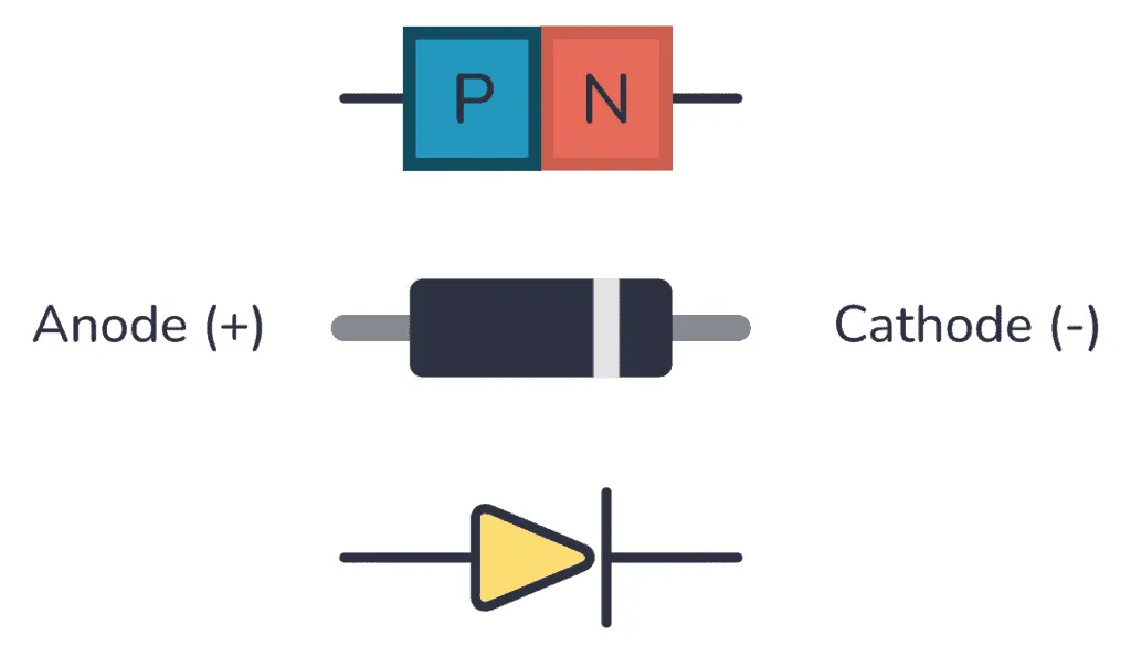
Body Diode Characteristics
Continuous diode forward current (IS): -0.13 A
Pulsed diode forward current (ISM): -0.52 A
Diode forward voltage (VSD): -2.2 V
Reverse recovery time (trr): xx ns
Reverse recovery charge (Qrr): xx uC
Characteristic Relationships
Transfer characteristic: With temperature constant, increasing VGS increases ID. At constant VGS, ID decreases as temperature rises.
Output characteristic: With voltage constant, increasing VDS increases ID. At constant VDS, ID increases with higher applied voltage.
RDS(on) vs ID: At constant temperature, RDS(on) increases slowly as ID increases. At constant ID, RDS(on) increases with temperature.
RDS(on) vs Tj: On the same curve, RDS(on) increases as Tj increases. On different curves, with higher Tj and larger ID, RDS(on) may appear smaller.
VDS vs parasitic capacitances: Increasing VDS reduces parasitic capacitances. Ciss is the largest, Coss is next, and Crss is the smallest.
Body diode VSD vs forward current IS: At constant temperature, -IS remains roughly stable following diode characteristics. At constant -VSD, -IS increases with temperature.