 ALLPCB


Overview
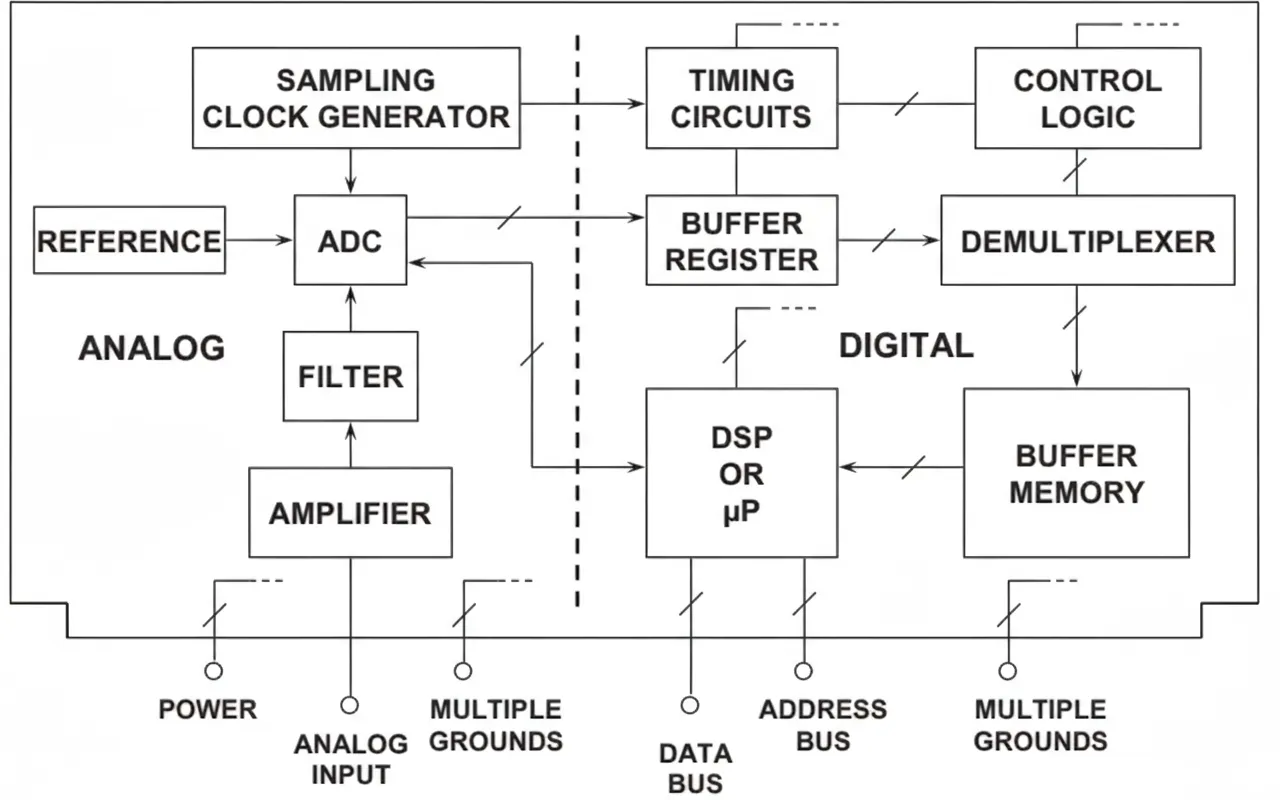
Modern signal processing systems commonly use mixed-signal devices such as analog-to-digital converters (ADC), digital-to-analog converters (DAC), and high-speed signal processors (DSP). To handle analog signals with wide dynamic range while preserving low noise, high-speed, high-performance circuit design techniques are required, including proper routing, decoupling, and grounding.
Historically, "high-precision, low-speed" analog circuits were treated differently from so-called "high-speed" circuits. For ADCs and DACs, sampling rate (for ADCs) and update rate (for DACs) have been used to classify speed. However, many modern signal-processing ICs operate with fast internal clocks and fast edges that make them effectively high-speed devices even if the throughput rate is modest. For example, a mid-speed 12-bit SAR ADC may run an internal clock at 10 MHz while the sample rate is only 500 kSPS. Sigma-delta ADCs also use high-frequency clocks due to high oversampling ratios. As mixed-signal ICs include both analog and digital pins, applying appropriate grounding techniques becomes more complex. Some mixed-signal ICs draw little digital current, while others draw substantial digital current; in many systems these two types must be treated differently to achieve optimal grounding.
Ground Plane and Return Path Fundamentals
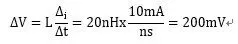
A low-impedance, large-area ground plane is essential for both analog and digital circuits. A continuous ground plane provides a low-impedance return path for high-frequency currents generated by fast digital logic and helps minimize EMI/RFI emissions. The plane also reduces sensitivity to external EMI/RFI and allows use of controlled-impedance transmission lines for high-speed digital or analog signals. Using wiring harnesses or single conductors as ground is unacceptable at logic-transition equivalent frequencies because the inductance creates significant voltage drops for fast current transients. For example, #22 wire has about 20 nH/inch inductance, so a transient current slew of 10 mA/ns across 1 inch produces about 200 mV of useless voltage drop, which could translate to a substantial error for analog signals.
Shared series inductance and resistance in the ground path produce cross-coupling that degrades accuracy. One possible approach is to route the digital return directly to a reference ground point, a star or single-point grounding concept. In practice, achieving a true single-point ground in systems with many high-frequency return paths is difficult because separate return conductors introduce parasitic inductance and resistance that violate the low-impedance requirement for high-frequency currents. At high frequencies, current loops must be formed by large-area ground planes to yield low impedance. Without a low-impedance ground plane it is nearly impossible to avoid shared impedance, especially at high frequency.
All IC ground pins should be tied directly to a low-impedance ground plane to minimize series inductance and resistance. For high-speed devices, traditional IC sockets are not recommended because added inductance and capacitance can introduce unwanted shared paths that degrade device performance. If sockets are required for DIP prototypes, use individual pin sockets or cage-type sockets with spring metal contacts to minimize additional parasitics, but be aware that repeated insertion/removal can reduce reliability.
Decoupling: Low-Frequency and High-Frequency
Each power input onto a PCB should be decoupled to the ground plane with bulk electrolytic (or similar) capacitors close to the power entry to suppress low-frequency noise on supply lines. Each local analog stage and IC power pin should also have local high-frequency bypassing using low-inductance ceramic capacitors sized for the frequencies of interest. Typical practice places 0.1 μF ceramic bypass capacitors close to IC power pins for frequencies up to roughly 20 MHz; higher frequencies require smaller-value, lower-inductance capacitors.
All high-speed ICs (clock frequencies greater than about 10 MHz) require bypassing. Ferrite beads are not always required but can improve isolation of high-frequency noise from power rails; verify that beads do not saturate during intended IC current transients, and check for nonlinear behavior prior to saturation if low-distortion power is required.
Two-layer and Multilayer PCBs
Every PCB should have at least one full plane reserved for ground. Ideally, a two-layer board would devote one side entirely to ground and the other to routing; in practice some ground area must be removed for signal and power crossings, vias, and through-hole pads, but ground area should be preserved as much as possible, with at least 75% retained where feasible. After initial placement, inspect the ground plane for isolated "islands" of copper that are not connected to the main ground plane; IC ground pins located on isolated islands will have no proper return path. Also verify that large adjacent ground areas are strongly connected to avoid reduced effectiveness of the ground plane. Manual routing is generally recommended for mixed-signal boards; automatic routing tools may not yield optimal mixed-signal layouts. Surface-mount, high-density systems typically require multi-layer boards so that a full internal layer can be dedicated to ground. A 4-layer board provides separate internal ground and power planes and outer signal layers, and placing power and ground planes adjacent creates interplane capacitance that aids high-frequency decoupling. Many systems need more than four layers to accommodate signal and power routing.
Multi-Board Mixed-Signal Systems
In multi-board systems the best way to reduce ground impedance between cards is to use a backplane PCB providing continuous ground planes for inter-card connections.
Two general grounding architectures are used in complex systems: 1) The backplane ground plane is connected to chassis ground at multiple points so that return currents are distributed; this is commonly called a multi-point ground system. 2) The ground plane is connected to a single system "star" ground point, typically near the power supply.
The first method is commonly used in fully digital systems but can be used in mixed-signal systems if digital return currents are low and distributed over a large area. Good electrical contact where the ground plane connects to the metal chassis is critical; use appropriate hardware to ensure low contact resistance. If the chassis finish is insulating (for example, anodized aluminum), special care is required because the chassis surface can be nonconductive.
The second method, the star ground, is often used in high-speed mixed-signal systems with separate analog and digital ground systems and merits further discussion below.
Related Reading: DFM Pitfalls to Avoid in Mixed-Signal PCB Layout
Physically Separating Analog and Digital Ground Planes
In systems with substantial digital circuitry, it is beneficial to separate sensitive analog components physically from noisy digital components and to provide separate analog and digital ground planes. Avoiding overlap between the analog and digital planes reduces capacitive coupling. Separate analog and digital ground planes can be continued through the backplane or ground mesh formed by connector ground pins and the backplane ground. As shown in the next figure, the two planes remain separate until they return to the system star ground, typically at the power supply. Connections between ground planes, power, and the star ground should use multiple wide straps or bus bars to minimize resistance and inductance. Insert back-to-back Schottky diodes at card insertion points to prevent unintended DC offsets between planes during hot-plug events; the DC offset should be kept below about 300 mV to avoid damaging ICs connected to both planes. Schottky diodes are preferred for their low forward drop and low capacitance; low capacitance minimizes AC coupling between analog and digital grounds. In some cases ferrite beads can be used instead of Schottky diodes, but beads provide a DC ground loop and may be problematic in precision systems.

Separated analog and digital ground planes. Ground-plane impedance must be minimized back to the system star ground. Any DC or low-frequency difference larger than about 300 mV between the planes can damage ICs or cause logic errors and latching.
Grounding and Decoupling for Mixed-Signal ICs with Low Digital Current
Sensitive analog components such as amplifiers and voltage references should always reference and decouple to the analog ground plane. Mixed-signal ICs with low digital currents, such as many ADCs and DACs, are generally best treated as analog devices and grounded and decoupled to the analog ground plane. Although converters have both analog and digital interfaces and often have pins labeled AGND and DGND, the external connection strategy matters. A simple converter model helps explain the reasoning.
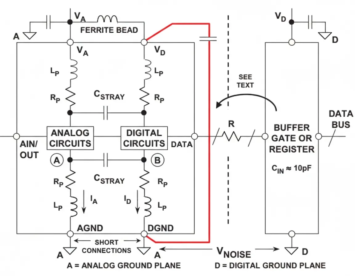
Within a mixed-signal IC, internal grounds are kept separate to avoid coupling digital signals into analog circuits. However, parasitic inductance and resistance between package pads and pins generate voltage at node B when digital currents change rapidly; stray capacitance between nodes couples some of that noise to the analog node A. To minimize this effect, AGND and DGND pins should be tied together externally with the shortest possible connection and returned to the analog ground plane. Any extra impedance in the DGND path increases digital noise at node B, which can couple via stray capacitance into the analog domain.
Note that labeling a pin "DGND" only identifies it as the device's digital ground internally; it does not mandate connecting that pin to the system digital ground plane. Connecting DGND to the analog ground plane can inject a small amount of digital noise into the analog plane, but if the converter's digital outputs are designed with small fan-out, those currents are typically small and manageable.
Minimizing fan-out from the converter's digital outputs reduces ringing and switching current and lowers the chance of coupling into the converter analog pins. Placing a small lossy ferrite bead in series with the converter digital supply pin (VD) isolates the logic supply from the analog supply, causing internal digital transient currents to circulate in a small local loop from VD through decoupling capacitors to DGND. Decoupling capacitors for the VD pin should be low-inductance ceramics placed as close as possible to the converter pins; values are commonly in the 0.01 μF to 0.1 μF range.
Handling ADC Digital Outputs
Placing buffer registers close to the converter is a good practice to isolate the converter digital lines from the main data bus. Buffers reduce the load on the converter outputs and provide Faraday shielding between the converter outputs and the data bus. Even if many converters provide tri-state outputs, isolation registers still represent good design practice. In some cases additional buffer registers mounted on the analog ground plane next to the converter outputs can provide better isolation.
A series resistor between the ADC outputs and buffer inputs (labeled R in Figure 5) helps limit digital transient currents that may affect converter performance. The resistor isolates the converter driver from the capacitive load of the buffer inputs; the RC formed by the resistor and input capacitance acts as a low-pass filter to slow edges. A typical CMOS gate combined with PCB traces and vias may present about 10 pF of load. Without series resistance, a 1 V/ns edge would create about 10 mA of dynamic current. Driving a 10 pF input through a 500 Ω series resistor reduces output current and produces approximately 11 ns rise/fall times.
TTL buffer registers have relatively high input capacitance and can significantly increase dynamic switching current and should be avoided in these applications. Buffer registers and other digital circuits should be grounded and decoupled to the board digital ground plane.
Any noise between analog and digital ground planes reduces the noise margin on the converter digital interface. Digital noise immunity is typically on the order of hundreds to thousands of millivolts, so small analog-ground noise is often acceptable. However, if the digital-to-analog ground potential difference exceeds a few hundred millivolts, reduce digital-ground impedance to keep the noise margin acceptable. Under no circumstances should the voltage between the two ground planes exceed about 300 mV, as this can damage ICs. It is also advisable to separate analog and digital power supplies, even if they have the same nominal voltage; the analog supply should power the converter analog sections. If the converter has a pin designated as the digital supply (VD), it should be powered from a filtered or separate supply as shown previously. All converter supply pins should be decoupled to the analog ground plane; logic supplies should be decoupled to the digital ground plane.
In some devices VD cannot be tied to the analog supply. Some high-speed ICs use +5 V for analog and +3 V for digital interfaces; in such cases the +3 V pin should be decoupled to the analog ground plane and a ferrite bead may be placed in series with the digital supply trace to the board +3 V. Sampling clock generators should be treated like analog circuits and grounded and decoupled to the analog ground plane, since clock phase noise degrades system SNR.
Sampling Clock Considerations
High-performance sampled-data systems require low-phase-noise oscillators for ADC or DAC sampling clocks. Clock jitter corrupts analog input/output and increases noise and distortion. The effect of sampling clock jitter on ADC SNR can be approximated by a formula that depends on the RMS clock jitter tj and the analog input frequency f. Using tj = 50 ps RMS and f = 100 kHz yields SNR around 90 dB (roughly 15 bits of dynamic range). In many high-performance ADCs, internal aperture jitter is negligible compared to external clock jitter.
Ideally the clock oscillator references the analog ground plane. In many systems the master clock originates on the digital ground plane and must be routed to the ADC on the analog ground plane; ground noise between the planes adds jitter to the clock and introduces spurious tones and SNR degradation. Transmitting the sampling clock as a differential signal using a small RF transformer or a high-speed differential driver/receiver pair can mitigate ground noise coupling, especially since many high-speed ADCs accept differential clock inputs. Use low-jitter differential standards such as ECL, low-voltage ECL, or LVDS to minimize phase noise. In single-supply +5 V systems, ECL variants such as PECL can be used with AC coupling into the ADC clock input. The original master system clock should come from a low-phase-noise oscillator rather than from DSP, microprocessor, or microcontroller clock outputs.
Why Grounding Guidance Can Be Confusing
Many ADC, DAC, and mixed-signal component datasheets describe grounding for a single PCB, often the manufacturer's own eval board. Applying those single-board recommendations to multi-board or multi-ADC/DAC systems can cause confusion. For single-PCB systems with a single converter, it is common to split the board ground into analog and digital planes and tie AGND and DGND together at one point where the two planes connect to create a local star ground. This approach often works for single-board systems but is not generally suitable for multi-board systems where analog and digital planes may connect at multiple points across multiple boards, creating ground loops. For that reason, a single-point star ground is not always practical in multi-board systems. The single-board star-ground approach applies primarily to mixed-signal ICs with low digital currents.
Related Reading: ADC and DAC Performance Metrics and Topologies
Grounding Mixed-Signal Devices with Low Digital Current in Multi-Board Systems
The approach for low-digital-current mixed-signal devices in multi-board systems. Small transient digital currents circulate in a small local loop from VD to DGND through decoupling, so the analog ground plane is preserved. Noise between ground planes reduces the noise margin on digital interfaces, but if the digital-plane impedance is kept low so that the plane-to-plane noise remains below roughly 300 mV and the connection returns to the system star ground, there is generally no adverse effect.
However, sigma-delta ADCs, codecs, and DSPs are increasingly digitally complex, and their internal digital currents can be substantial due to on-chip digital filters and other logic. If the internal digital currents are large or have DC or low-frequency components, relying on decoupling between VD and DGND may be inadequate because decoupling cannot handle large DC currents. Any digital current that flows outside the small loop will traverse the analog ground plane and may degrade performance in high-resolution systems. Predicting the threshold of unacceptable digital current in the analog ground is difficult, so alternatives are recommended.
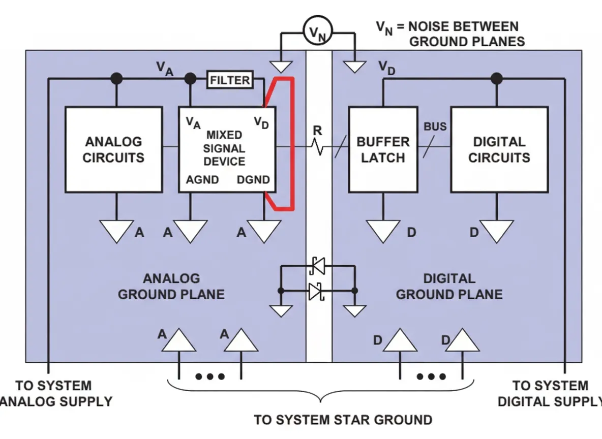
Grounding Mixed-Signal Devices with High Digital Current in Multi-Board Systems
For mixed-signal ICs with high digital currents, an alternative grounding scheme. Connect AGND to the analog ground plane and DGND to the digital ground plane. Digital currents are thus isolated from the analog plane, but noise between planes appears directly across the AGND and DGND pins. For this method to succeed, the IC must have good internal isolation between analog and digital domains so that plane-to-plane noise does not reduce internal margins or damage analog circuitry.
Options to connect the analog and digital planes include back-to-back Schottky diodes or ferrite beads. Back-to-back Schottky diodes prevent large DC or low-frequency spikes between planes; if the voltage across AGND and DGND exceeds roughly 300 mV, the diodes conduct, protecting the IC. Ferrite beads provide a DC connection while isolating at higher frequencies; because beads become resistive above a few MHz, they allow isolation of high-frequency noise but create a DC connection that may form unwanted ground loops and may be unsuitable for very high-resolution systems. When AGND and DGND pins are separated internally in devices with high digital currents, experiment with tying them together using jumpers or straps to evaluate which approach yields the best system performance.
Grounding Summary
There is no single grounding method that guarantees optimal performance in every situation. The recommendations in this article present several viable options depending on device characteristics. When implementing an initial PCB layout, provide choices so you can experiment during validation—for example, include pads and vias for connecting analog and digital ground planes with jumpers, ferrite beads, or back-to-back Schottky diodes. Ensure the PCB has at least one layer dedicated to ground. Begin with non-overlapping analog and digital ground planes, and include pads and vias to install components for joining or isolating the planes as needed. Because it is difficult to predict whether a single-plane (multi-point) or star-ground approach will perform best, the ability to reconfigure ground connections on the final PCB is valuable. If unsure, start with separate analog and digital ground planes and add jumpers later as needed rather than starting with a single plane and later trying to separate it.
General PCB Layout Guidelines for Mixed-Signal Systems
Careful planning of system layout and minimizing interactions between signals reduces noise. High-amplitude analog signals should be separated from low-level analog signals, and both should be kept away from digital signals. Sampling clocks are as susceptible to noise as analog signals and can also generate noise, so clocks should be isolated from both analog and digital systems. If a clock driver package distributes multiple clock frequencies, avoid sharing the driver among different-frequency clocks because it increases jitter and crosstalk. Ground planes serve as shields where sensitive signals cross.
Consider connector placement carefully: connectors are locations where multiple signal transmission lines run in parallel and therefore require ground pins between signal pins to form a Faraday shield that reduces coupling. Multiple connector ground pins also lower the contact impedance between boards and the backplane. On new PCBs connector contact resistance is low but may increase with age and wear, so allocating many ground pins is prudent. Typically 30–40% of connector pins should be ground. Each power connection should use multiple pins, although not as many as ground pins.
High-performance mixed-signal IC vendors provide evaluation boards that assist with initial evaluation and layout. ADC evaluation boards often include low-jitter sampling clock oscillators, output registers, and appropriate power and signal connectors, along with support circuits such as input buffers and external references. Evaluation board layouts are optimized for grounding, decoupling, and signal routing and can serve as a template for system boards; many vendors supply the layered PCB files or Gerber data for study.


