ALLPCB


If you're involved in PCB design or manufacturing, you might wonder how tolerances in controlled depth drilling, often referred to as back drilling, affect the final product. Simply put, tolerances in controlled depth drilling are critical because they determine the accuracy of removing unused via stubs, ensuring signal integrity, especially in high-speed circuits. Poor tolerances can lead to manufacturing variations, signal loss, or even board failure. In this blog, we'll dive deep into the significance of PCB tolerances, back drilling accuracy, and the design considerations you need to keep in mind to avoid costly errors and achieve optimal performance.
Understanding Controlled Depth Drilling and Its Importance in PCB Manufacturing
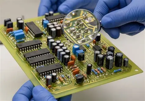
Controlled depth drilling, commonly known as back drilling, is a specialized technique used in multilayer PCB manufacturing. It involves drilling into a via from the opposite side of the board to remove the unused portion of the copper barrel, also called a stub. These stubs, if left in place, can act as antennas, causing signal reflections and degrading performance in high-speed applications.
Back drilling is especially vital for designs operating at signal speeds above 3 Gbps, where even small stubs can introduce significant noise. By precisely controlling the depth of the drill, manufacturers can eliminate these stubs without damaging the functional part of the via. However, achieving this precision depends heavily on maintaining tight PCB tolerances during the drilling process.
What Are PCB Tolerances and Why Do They Matter?
PCB tolerances refer to the acceptable range of deviation in manufacturing processes, such as drilling, routing, or plating. They define the upper and lower limits within which a feature, like a drilled hole or via depth, must fall to ensure the board functions as intended. In the context of controlled depth drilling, tolerances directly impact back drilling accuracy and, ultimately, the board's performance.
For instance, a typical tolerance for back drilling depth might be ±0.05 mm. If the drill goes too deep, it risks damaging the functional via barrel, leading to connectivity issues. If it’s too shallow, a residual stub remains, causing signal integrity problems. Maintaining tight tolerances is essential to avoid these manufacturing variations and ensure consistent quality across production runs.
Tolerances also affect other aspects of PCB manufacturing, such as copper thickness and hole positioning. A variation in copper thickness, for example, can alter impedance values, which are critical for high-speed signals. Standard impedance tolerances are often ±10%, but for high-precision designs, this might need to be tightened to ±5% or less, depending on the application.
How Back Drilling Accuracy Affects Signal Integrity
In high-speed PCB designs, signal integrity is everything. When signals travel through vias with unused stubs, they can reflect back, creating noise and distortion. This is particularly problematic for applications like telecommunications or data centers, where data rates often exceed 10 Gbps. Back drilling accuracy ensures that these stubs are removed with precision, minimizing reflections and maintaining clean signal paths.
The accuracy of back drilling is tied to the capabilities of modern numerically controlled (NC) drilling equipment. These machines can achieve depth precision within ±0.05 mm, but only if the design files specify exact depths and tolerances are strictly followed. Even a small deviation of 0.1 mm in drilling depth can result in a stub long enough to cause a measurable impact on signal performance at high frequencies.
Manufacturing Variations: Challenges in Controlled Depth Drilling
Manufacturing variations are inevitable in PCB production, but they can be minimized with proper planning and tight tolerances. In controlled depth drilling, variations can arise from several factors, including equipment limitations, material inconsistencies, and human error. Let’s break down some of these challenges:
- Equipment Precision: Not all drilling machines are created equal. Older equipment may struggle to maintain the tight tolerances required for back drilling, leading to inconsistent depths across the board.
- Material Properties: Variations in PCB material thickness or hardness can affect how the drill behaves. For example, a harder laminate might cause the drill to deflect slightly, impacting accuracy.
- Layer Alignment: In multilayer boards, misalignment between layers can result in incorrect drilling depths, as the drill may not target the intended via stub accurately.
To mitigate these variations, manufacturers often use advanced inspection tools like X-ray systems to verify drilling accuracy post-production. Additionally, specifying clear PCB specifications in design files can help ensure that the manufacturing process aligns with the intended outcome.
Design Considerations for Controlled Depth Drilling
Designing a PCB for controlled depth drilling requires careful attention to detail. Here are some key design considerations to ensure back drilling accuracy and minimize manufacturing variations:
1. Specify Exact Drilling Depths
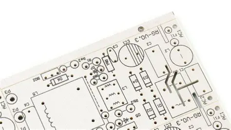
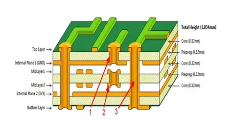
Your design files should include precise depth specifications for back drilling. This information guides the NC drilling equipment to achieve the desired results. For instance, if a via connects layers 1 to 4 in a 12-layer board, the back drilling depth should be calculated to remove the stub from layers 5 to 12 without affecting the functional barrel.
2. Focus on High-Speed Vias
Not all vias need back drilling. Prioritize vias that carry high-speed signals, typically above 3 Gbps, where signal integrity is critical. Power and ground vias, or those used for low-speed signals, often don’t require this process, saving time and cost in manufacturing.
3. Account for Tolerances in Design
When defining via sizes and drilling depths, consider the tolerances of the manufacturing process. For example, if the drilling tolerance is ±0.05 mm, ensure that your design can accommodate this variation without compromising functionality. Adding a small buffer in the via stub length can help prevent issues if the drill is slightly off.
4. Collaborate with Your Manufacturer
Every manufacturing facility has its own capabilities and limitations. Early collaboration with your manufacturer can help align your design with their equipment and process tolerances. Share detailed PCB specifications and discuss any critical requirements, such as impedance control or specific drilling depths, to avoid surprises during production.
The Role of PCB Specifications in Minimizing Errors
Clear and detailed PCB specifications are the foundation of a successful manufacturing process. These specs act as a blueprint for the manufacturer, ensuring that every aspect of the board, from drilling depths to copper thickness, meets the design requirements. In the context of controlled depth drilling, specifications should include:
- Exact via locations and depths for back drilling.
- Tolerance limits for drilling accuracy, such as ±0.05 mm.
- Signal speed requirements to identify which vias need back drilling.
- Material stack-up details to account for variations in layer thickness.
By providing comprehensive specifications, you reduce the risk of miscommunication and manufacturing errors. This is particularly important for complex designs with tight tolerances, where even a small deviation can lead to significant performance issues.
Practical Tips for Achieving Tight Tolerances in Back Drilling
If you're aiming for high back drilling accuracy, here are some actionable tips to help you succeed:
- Use Advanced Design Software: Leverage PCB design tools that allow you to simulate signal integrity and specify precise drilling depths. These tools can help identify potential issues before manufacturing begins.
- Opt for High-Quality Materials: Consistent material properties reduce variations during drilling. Choose laminates with stable thickness and hardness to ensure uniform results.
- Request Post-Drilling Inspection: Ask your manufacturer to perform X-ray or automated optical inspection (AOI) to verify drilling depths and ensure compliance with tolerances.
- Test Prototypes: Before full-scale production, create and test prototypes to validate your design and manufacturing process. This step can uncover hidden issues with tolerances or back drilling accuracy.
The Cost Implications of Tolerances in Controlled Depth Drilling
Maintaining tight tolerances in controlled depth drilling often comes with a cost. Advanced NC drilling equipment, precise inspection methods, and additional quality control steps can increase production expenses. However, the investment is often worth it for high-speed applications where signal integrity is non-negotiable.
For lower-speed designs, you might be able to relax tolerances and skip back drilling for certain vias, reducing costs without sacrificing performance. The key is to strike a balance between precision and affordability, tailoring your approach based on the specific requirements of your project.
Conclusion: Mastering Tolerances for Better PCB Performance
Tolerances in controlled depth drilling play a pivotal role in ensuring the quality and reliability of modern PCBs, especially for high-speed applications. By understanding the impact of PCB tolerances, prioritizing back drilling accuracy, and addressing manufacturing variations through careful design considerations, you can achieve superior signal integrity and avoid costly errors.
Whether you're specifying exact drilling depths or collaborating with your manufacturer to align on PCB specifications, every step counts. With the right approach, you can navigate the challenges of controlled depth drilling and deliver boards that meet the highest standards of performance. Keep these insights in mind as you design your next project, and you'll be well-equipped to handle the complexities of modern PCB manufacturing.