ALLPCB


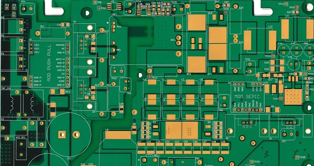
In the world of PCB design, achieving the right copper balance is crucial for ensuring optimal electrical performance and signal integrity. But what exactly is copper balance, and why does it matter for PCB manufacturing? In short, copper balance refers to the even distribution of copper across the layers of a printed circuit board (PCB) to prevent warping, ensure uniform plating, and maintain reliable electrical performance. This blog dives deep into the importance of copper balance in PCB design, its impact on electrical performance and signal integrity, and actionable tips for optimizing your designs during manufacturing.
Whether you’re an engineer working on high-speed circuits or a designer aiming for flawless PCB production, understanding copper balance can make or break your project. Let’s explore how to master this balancing act for better PCB electrical performance and manufacturing outcomes.
What Is Copper Balance in PCB Design?
Copper balance in PCB design refers to the uniform distribution of copper material across the layers of a printed circuit board. During the manufacturing process, copper is etched away to create traces, pads, and other features. If the copper isn’t distributed evenly, it can lead to uneven stress, warping, or inconsistent plating, all of which negatively affect the board’s performance and reliability.
Think of a PCB as a sandwich of materials, with copper layers acting as the bread. If one side has significantly more copper than the other, the board can bend or twist during fabrication due to thermal expansion or mechanical stress. This imbalance also impacts electrical performance by creating uneven current distribution, which can degrade signal integrity—especially in high-speed designs where precision is key.
Maintaining copper balance isn’t just about avoiding physical defects; it’s also about ensuring consistent electrical characteristics across the board. For example, uneven copper can lead to variations in impedance, which might cause signal reflections and data loss in high-frequency applications operating at speeds above 1 GHz.
Why Copper Balance Matters for PCB Electrical Performance
Copper balance plays a critical role in determining the electrical performance of a PCB. Here’s how an imbalance can impact your design:
- Impedance Control: In high-speed designs, maintaining consistent impedance is vital for signal integrity. If copper distribution varies, it can alter the characteristic impedance of traces, leading to signal reflections. For instance, a target impedance of 50 ohms for a differential pair might deviate to 55 or 60 ohms due to uneven copper, causing signal distortion.
- Current Distribution: Uneven copper can result in hotspots where current density is higher, leading to potential overheating or even component failure. Balanced copper ensures that current flows uniformly, reducing the risk of thermal issues.
- Electromagnetic Interference (EMI): Imbalanced copper can create unintended ground plane gaps or uneven reference planes, increasing EMI. This is especially problematic in high-frequency designs where EMI can disrupt nearby circuits or violate regulatory standards.
By prioritizing copper balance, designers can achieve stable electrical performance, ensuring that signals travel without distortion and power delivery remains consistent across the board.
The Impact of Copper Balance on Signal Integrity
Signal integrity is the measure of how well a signal maintains its quality as it travels through a PCB. Poor copper balance directly affects signal integrity, especially in high-speed applications where data rates can exceed 10 Gbps. Here’s how:
- Crosstalk: Uneven copper distribution can lead to inconsistent spacing between traces and ground planes, increasing crosstalk between adjacent signals. This interference can corrupt data, particularly in densely packed designs.
- Signal Delay: Variations in copper thickness or distribution can alter the dielectric properties around traces, causing unexpected delays in signal propagation. This is critical for timing-sensitive applications like DDR memory interfaces.
- Reflections and Loss: As mentioned earlier, impedance mismatches from uneven copper cause signal reflections, while excessive copper removal in some areas can increase resistive losses, degrading signal strength.
To maintain signal integrity, copper balance must be considered from the initial design stages. Tools like simulation software can predict potential issues by modeling impedance and signal behavior based on copper distribution, allowing designers to make adjustments before fabrication.
Copper Balance in PCB Manufacturing: Challenges and Solutions
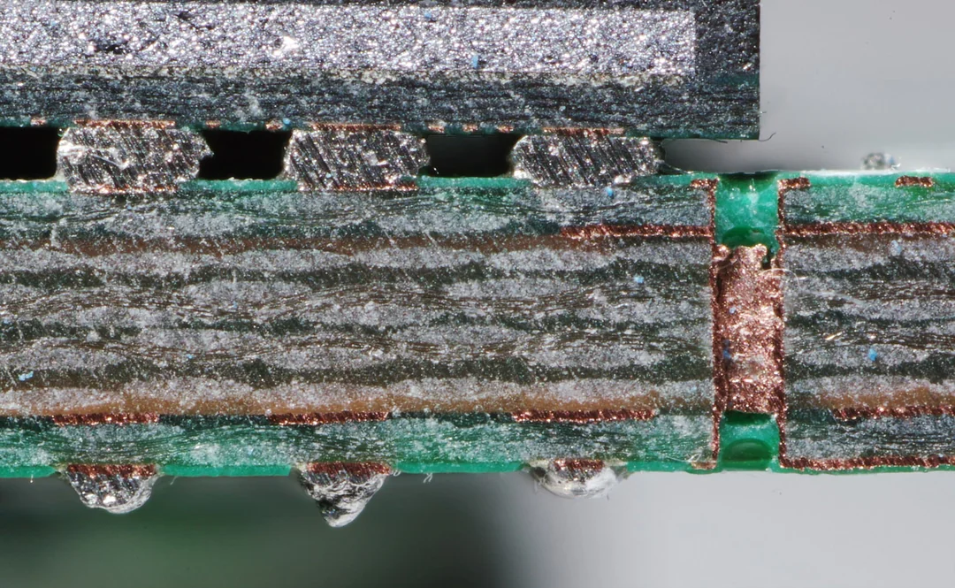
During PCB manufacturing, achieving copper balance presents several challenges. The etching process, for example, removes copper selectively to form traces and pads. If one area of the board has significantly less copper than another, the etching rate can vary, leading to over-etching or under-etching. This inconsistency affects not only the board’s physical structure but also its electrical performance.
Another common issue is warping during lamination. When copper distribution is uneven, the board experiences unequal thermal expansion as it undergoes heat and pressure, resulting in a bowed or twisted PCB. A warped board can cause assembly issues, such as misaligned components or poor soldering, ultimately reducing yield rates.
Fortunately, there are practical solutions to these manufacturing challenges:
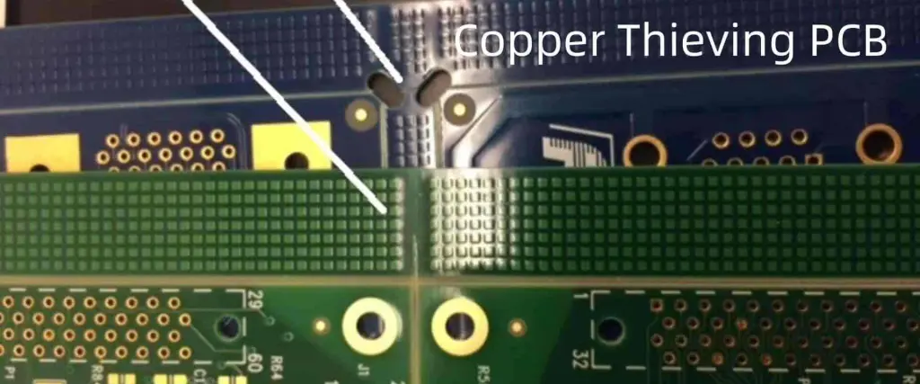
- Copper Thieving: This technique involves adding non-functional copper patterns, often in the form of small dots or grids, to areas with low copper density. These “thieves” balance the copper distribution, ensuring uniform plating and etching. For instance, if a board has a large empty space on one layer, adding a grid of copper dots can bring the density closer to that of busier areas.
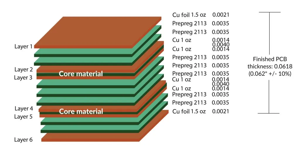
- Symmetrical Layer Stackup: Designing the PCB with symmetrical copper layers helps maintain balance across the board. For a 4-layer PCB, ensure that the top and bottom layers have similar copper coverage, as do the inner layers.
- Design Rule Checks (DRC): Use design software to run DRCs that flag areas of uneven copper density. Addressing these issues early prevents costly revisions during manufacturing.
By incorporating these strategies, manufacturers can minimize defects and produce boards that meet both physical and electrical performance standards.
Best Practices for Optimizing Copper Balance in PCB Design
Now that we’ve covered the importance of copper balance for electrical performance and manufacturing, let’s look at actionable best practices to optimize your PCB design:
- Plan Copper Distribution Early: During the schematic and layout phases, aim for even copper distribution across all layers. Avoid large empty spaces by filling them with non-functional copper or ground planes.
- Use Ground and Power Planes: Full copper planes for ground and power not only improve signal integrity by providing a low-impedance return path but also help balance copper across layers. For example, a solid ground plane can add necessary copper density to a layer with sparse traces.
- Match Copper Thickness: Ensure that the copper thickness (e.g., 1 oz or 2 oz per square foot) is consistent across layers unless specific performance requirements dictate otherwise. Variations in thickness can exacerbate imbalance.
- Simulate and Test: Use simulation tools to model the electrical and thermal behavior of your design. Testing prototypes under real-world conditions can also reveal copper balance issues before mass production.
- Collaborate with Fabricators: Work closely with your manufacturing partner to understand their specific requirements for copper balance. Some fabricators may have unique guidelines or capabilities that influence design decisions.
Implementing these practices can significantly enhance the reliability and performance of your PCB, reducing the likelihood of costly redesigns or production delays.
How Copper Balance Affects High-Speed PCB Designs
High-speed PCB designs, such as those used in telecommunications, automotive radar, or data centers, are particularly sensitive to copper balance. At frequencies above 1 GHz or data rates exceeding 5 Gbps, even minor imbalances can lead to significant performance degradation.
For instance, in a high-speed differential pair, uneven copper can cause skew between the positive and negative signals, leading to timing errors. Similarly, an unbalanced ground plane might fail to provide a proper return path, increasing loop inductance and EMI.
To address these challenges in high-speed designs, consider the following:
- Tight Impedance Control: Use controlled impedance traces and ensure copper balance to maintain a consistent 50-ohm or 100-ohm impedance for single-ended or differential signals, respectively.
- Via Stitching: Add via stitching around high-speed signals to connect ground planes, ensuring a uniform reference plane and reducing EMI caused by copper imbalance.
- Material Selection: Choose PCB materials with stable dielectric constants (e.g., FR-4 with a Dk of 4.2-4.5) to complement copper balance efforts, as material inconsistencies can compound electrical issues.
By focusing on copper balance, high-speed PCB designers can achieve the precision needed for cutting-edge applications.
Conclusion: Mastering the Copper Balancing Act
Copper balance is a fundamental aspect of PCB design that directly influences electrical performance, signal integrity, and manufacturing success. By ensuring even copper distribution across layers, designers can prevent physical defects like warping, maintain consistent impedance for signal integrity, and avoid thermal or EMI issues that compromise performance.
From using copper thieving and symmetrical stackups to leveraging simulation tools and collaborating with fabricators, there are numerous strategies to achieve optimal copper balance. Whether you’re working on a simple single-layer board or a complex high-speed design, prioritizing copper balance will lead to more reliable, high-performing PCBs.
At ALLPCB, we understand the intricacies of PCB design and manufacturing. Our expertise and advanced tools can help you navigate the copper balancing act, ensuring your designs meet the highest standards of electrical performance. Start optimizing your PCB designs today for better outcomes tomorrow.