ALLPCB


If you're a hobbyist looking to create custom circuit boards at home, mastering the PCB etching process is a must. Etching removes unwanted copper from a clad board to form your desired circuit traces. In this guide, we’ll walk you through the entire homemade PCB etching process using ferric chloride as a copper etchant, ensuring you can achieve professional results with minimal tools. Whether you're new to PCB fabrication for hobbyists or refining your skills, this step-by-step tutorial will cover everything you need to know about ferric chloride etching and more.
Introduction to PCB Etching for Hobbyists
Printed Circuit Boards (PCBs) are the backbone of modern electronics, and creating them at home is an exciting and cost-effective way to bring your projects to life. The PCB etching process involves selectively removing copper from a copper-clad board to leave behind the conductive traces that connect your components. For hobbyists, homemade PCB etching is a practical skill that allows for quick prototyping without the wait time or expense of professional manufacturing.
In this comprehensive guide, we’ll focus on using ferric chloride as a copper etchant—a popular choice due to its availability and effectiveness. We’ll break down each step of the process, from designing your circuit to safely handling chemicals, ensuring you can achieve clean and precise results. Let’s dive into the art of etching and transform a blank copper board into a functional PCB!
What You’ll Need for Homemade PCB Etching
Before starting, gather all necessary materials and tools to ensure a smooth workflow. Here’s a detailed list tailored for hobbyists embarking on PCB fabrication:
- Copper-Clad Board: Typically, a single or double-sided board with a copper thickness of 1 oz per square foot (about 35 micrometers) is ideal for most hobby projects.
- Ferric Chloride Solution: This is the primary copper etchant for the PCB etching process. It’s widely available in liquid or powder form (to be mixed with water).
- Protective Gear: Safety goggles, chemical-resistant gloves, and an apron to protect against splashes during ferric chloride etching.
- Etching Container: A non-metallic tray or plastic container to hold the etchant solution. Avoid metal as it reacts with ferric chloride.
- Masking Material: Toner transfer paper or photoresist film to create a protective layer over the copper traces you want to keep.
- Laser Printer or UV Light Source: For transferring your circuit design onto the board (depending on your masking method).
- Drill or Cutting Tools: For creating holes or trimming the board after etching.
- Cleaning Supplies: Acetone or rubbing alcohol, scrub pads, and paper towels for pre- and post-etching cleanup.
- Agitation Tool: A small brush or sponge to speed up the etching process (optional but recommended).
Understanding the PCB Etching Process
The PCB etching process is a chemical reaction where a copper etchant, like ferric chloride, dissolves the exposed copper on your board while leaving protected areas intact. Ferric chloride (FeCl?) reacts with copper to form copper chloride and iron compounds, effectively removing the metal from unprotected regions. The reaction is relatively fast, often completing in 10-30 minutes depending on temperature, concentration, and agitation.
For hobbyists, ferric chloride etching is preferred because it’s affordable, accessible, and works well at room temperature (around 20-25°C or 68-77°F). However, it’s crucial to handle this chemical with care as it’s corrosive and can stain surfaces or irritate skin.
Step-by-Step Guide to Homemade PCB Etching
Now, let’s walk through the detailed steps of PCB fabrication for hobbyists using ferric chloride as the copper etchant. Follow these instructions carefully for the best results.
Step 1: Design Your Circuit
Start by creating your circuit layout using design software. Print the design onto toner transfer paper using a laser printer, ensuring the traces are mirrored if you’re working on the bottom side of the board. The black toner will act as a resist during the etching process, protecting the copper beneath it.
Tip: Aim for trace widths of at least 0.25 mm (10 mils) to ensure reliability, especially for high-current paths. For signal integrity, maintain consistent spacing to avoid crosstalk—0.3 mm (12 mils) is a safe minimum for most low-speed designs.
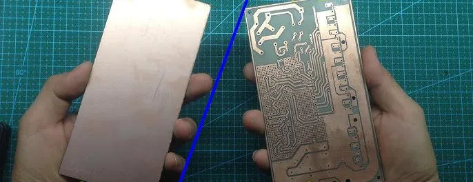
Step 2: Prepare the Copper-Clad Board
Clean the copper surface thoroughly to remove oxidation and fingerprints, which can interfere with toner transfer or photoresist adhesion. Use a scrub pad or fine sandpaper to lightly abrade the surface, then wipe it down with acetone or rubbing alcohol. A shiny, uniform copper surface ensures better results during the PCB etching process.
Step 3: Transfer the Design to the Board
Place the printed toner transfer paper face down on the copper board. Use an iron set to high heat (no steam) to transfer the toner onto the copper by pressing firmly for 2-5 minutes. Once cooled, soak the board in water for 10 minutes to loosen the paper, then gently peel it off. Inspect the toner for any breaks or smudges and repair them with a permanent marker if needed.
If using photoresist film, apply it to the board, expose it to UV light through a printed transparency of your design, and develop it according to the manufacturer’s instructions.
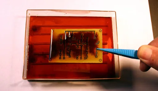
Step 4: Set Up for Ferric Chloride Etching
Work in a well-ventilated area and wear protective gear. Pour the ferric chloride solution into a non-metallic container—use just enough to submerge the board (typically 200-500 ml for small boards). Warm the solution to around 35-40°C (95-104°F) to speed up the reaction, but avoid exceeding 50°C (122°F) as it can produce harmful fumes.
Safety Note: Ferric chloride is corrosive. Avoid skin contact and never pour it down the drain—store used solution for proper disposal according to local regulations.
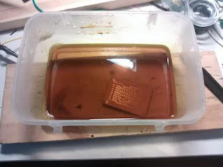
Step 5: Etch the Board
Place the board into the ferric chloride solution, copper side up. Agitate the solution gently by rocking the container or using a small brush to speed up the process and ensure even etching. Check the board every 5 minutes—etching typically takes 10-30 minutes depending on the copper thickness and solution strength. You’ll see the exposed copper dissolve, leaving behind the protected traces.
Tip: If etching takes longer than 30 minutes, the solution may be too weak or cold. Consider refreshing the etchant or increasing the temperature slightly.
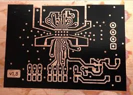
Step 6: Rinse and Clean the Board
Once all exposed copper is removed, carefully lift the board out of the solution using tongs or gloved hands. Rinse it under running water to stop the etching process. Remove the toner or photoresist using acetone or a scrub pad to reveal the clean copper traces underneath. Dry the board with a paper towel.
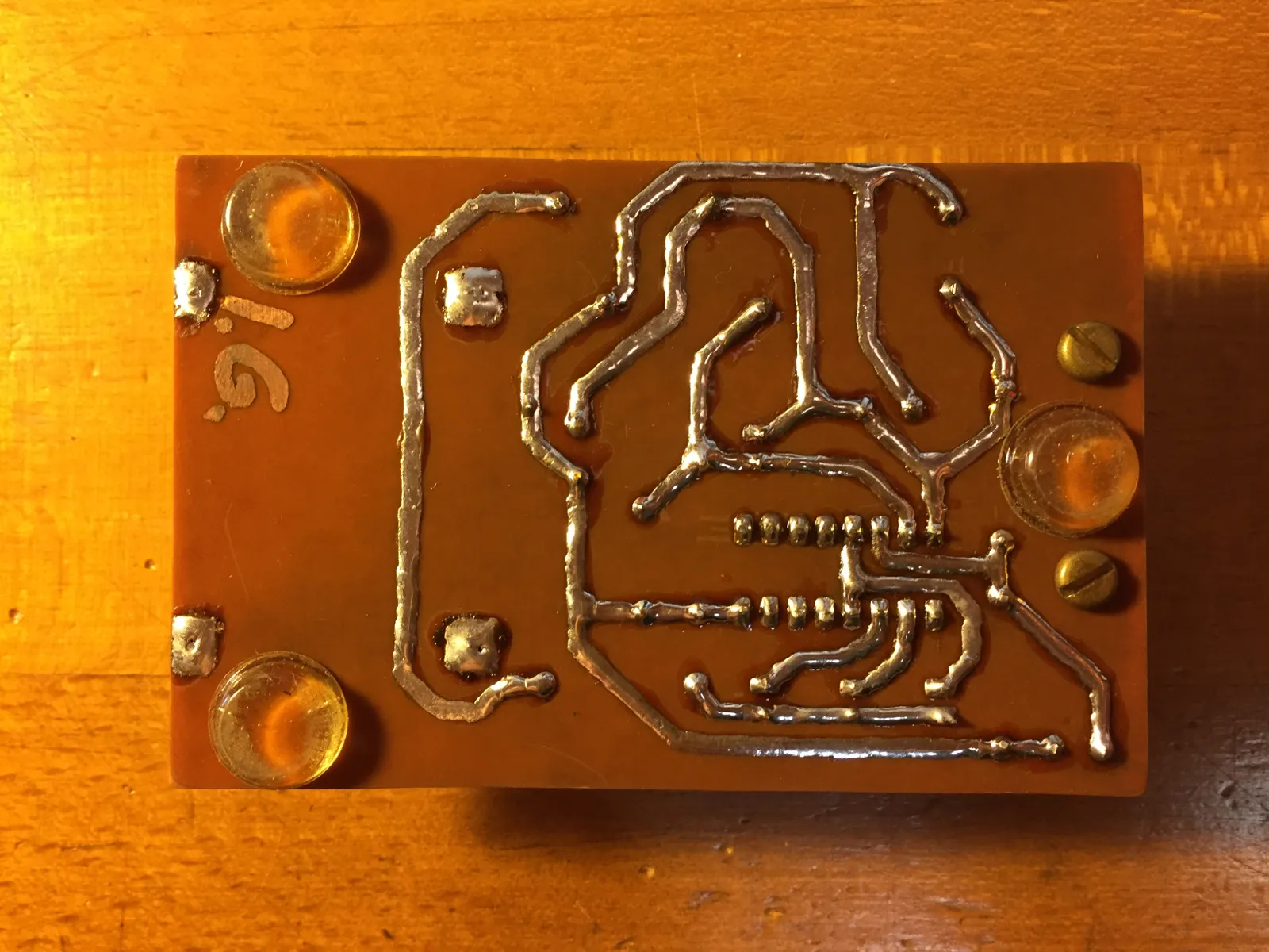
Step 7: Inspect and Finish
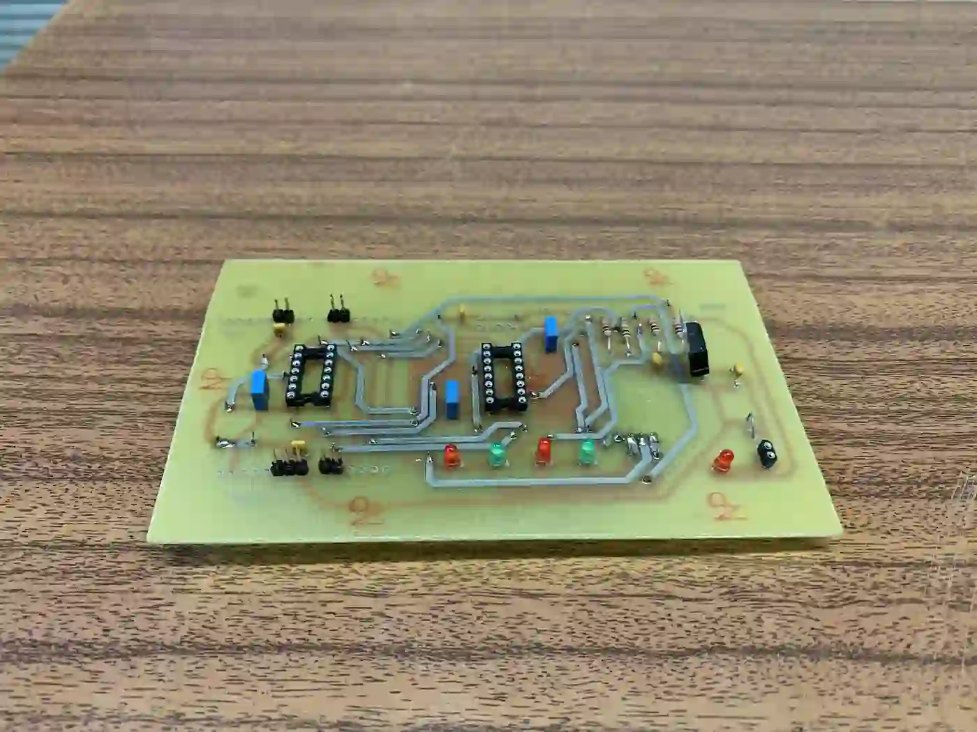
Inspect the board for any under-etched areas (where copper remains) or over-etched traces (where copper is unintentionally removed). If needed, touch up with a small amount of etchant or redo the process for problem areas. Finally, drill holes for components using a small drill bit (0.8-1.2 mm for standard through-hole components) and trim the board to size if necessary.
Safety Tips for Ferric Chloride Etching
Handling chemicals during homemade PCB etching requires caution. Follow these safety guidelines to protect yourself and your workspace:
- Always wear safety goggles and chemical-resistant gloves when working with ferric chloride.
- Work in a well-ventilated area to avoid inhaling fumes, especially if the solution is heated.
- Store ferric chloride in a labeled, sealed container away from children and pets.
- Never mix ferric chloride with other chemicals unless you’re certain of the reaction—unexpected byproducts can be dangerous.
- Dispose of used etchant responsibly. Contact local waste management for guidance on hazardous chemical disposal.
Troubleshooting Common Issues in PCB Etching
Even with careful preparation, issues can arise during the PCB etching process. Here are solutions to common problems faced by hobbyists:
- Under-Etching (Copper Not Fully Removed): This can happen if the etchant is too weak or cold. Warm the solution to 35-40°C or replace it with a fresh batch. Agitation also helps.
- Over-Etching (Traces Damaged): If traces are too thin or broken, reduce etching time or check toner transfer for incomplete coverage. Use a marker to reinforce weak spots before etching.
- Uneven Etching: Ensure consistent agitation and avoid air bubbles on the board surface, which can block the etchant.
- Poor Toner Transfer: If the design doesn’t adhere properly, clean the copper more thoroughly or increase ironing time and pressure.
Alternative Copper Etchants for Hobbyists
While ferric chloride etching is the go-to method for many, other copper etchants are available for homemade PCB etching. Here are two alternatives:
- Hydrogen Peroxide and Hydrochloric Acid: Mix equal parts of 3% hydrogen peroxide and 30% hydrochloric acid (muriatic acid). This solution etches quickly (often under 10 minutes) but requires extra caution due to stronger fumes and corrosiveness.
- Vinegar and Hydrogen Peroxide: A slower, safer option using household items. Mix equal parts white vinegar (5% acetic acid) and 3% hydrogen peroxide. This method can take several hours and is less reliable for fine traces but produces fewer harmful fumes.
Stick with ferric chloride if you’re new to PCB fabrication for hobbyists, as it offers a good balance of speed, control, and availability.
Environmental Considerations and Disposal
The PCB etching process involves chemicals that can harm the environment if not handled properly. Used ferric chloride contains dissolved copper, making it toxic to aquatic life. Never pour it down the drain or into the soil. Instead, store it in a sealed, labeled container and take it to a hazardous waste disposal facility. Some regions allow small amounts to be neutralized with baking soda before disposal—check local regulations for specifics.
Conclusion: Mastering the Art of PCB Etching
Homemade PCB etching is a rewarding skill that opens up endless possibilities for hobbyists. By following this step-by-step guide to copper cladding removal using ferric chloride etching, you can create custom circuit boards with precision and confidence. From designing your circuit to safely handling copper etchant, each stage of the PCB etching process builds your expertise in PCB fabrication for hobbyists.
Remember to prioritize safety, troubleshoot issues as they arise, and dispose of chemicals responsibly. With practice, you’ll refine your technique and produce professional-quality PCBs right from your workshop. Start small, experiment with different methods, and watch your electronics projects come to life!