If you're looking for standard PCB dimensions for LED lighting applications, the answer depends on the specific use case, power requirements, and design constraints. While there are no universally fixed dimensions, common sizes for LED PCBs often range from small modules (20mm x 20mm for compact lighting) to larger panels (up to 500mm x 500mm for industrial or street lighting). Design considerations like thermal management, component placement, and high-power needs play a critical role in determining the ideal size and layout. In this comprehensive guide, we'll dive deep into LED PCB design guidelines, thermal management in LED PCBs, LED component placement, high-power LED PCB design, and standard PCB dimensions for LED lighting to help you create efficient and reliable designs.
Introduction to LED PCB Design for Lighting Applications
LED lighting has revolutionized the way we illuminate spaces, offering energy efficiency, long lifespan, and versatility. However, designing a printed circuit board (PCB) for LED applications requires careful planning to ensure optimal performance. The size of the PCB, placement of components, and heat dissipation strategies are just a few of the factors that can make or break your design. Whether you're working on residential lighting, automotive systems, or industrial solutions, understanding standard PCB dimensions for LED lighting and key design principles is essential for success.
In this blog, we'll explore the best practices for designing LED PCBs, focusing on practical tips and actionable insights. From choosing the right dimensions to managing heat in high-power setups, we've got you covered with detailed guidance tailored for engineers and designers.
Understanding Standard PCB Dimensions for LED Lighting
One of the first questions in LED PCB design is, "What are the standard dimensions for my application?" While there’s no one-size-fits-all answer, certain dimensions are commonly used based on the type of lighting product. Here's a breakdown:
- Small LED Modules: Often used in compact lighting like bulbs or indicator lights, these PCBs can be as small as 20mm x 20mm. They typically support a few LEDs and are ideal for low-power applications.
- Strip Lighting PCBs: For flexible or linear LED strips, dimensions are often long and narrow, such as 500mm x 10mm. These are common in decorative or under-cabinet lighting.
- Medium Panels: Used in downlights or panel lights, these PCBs might measure around 100mm x 100mm to 300mm x 300mm, depending on the number of LEDs and power needs.
- Large Industrial Boards: For high-power applications like streetlights or floodlights, PCBs can reach up to 500mm x 500mm or larger to accommodate numerous LEDs and heat dissipation components.
Choosing the right dimensions involves balancing space constraints with performance needs. Smaller PCBs are cost-effective but may struggle with heat dissipation in high-power setups. Larger boards offer more room for components and thermal management but increase manufacturing costs. Always consider the enclosure size, mounting requirements, and electrical specifications when deciding on PCB dimensions.
Key LED PCB Design Guidelines for Optimal Performance
Designing a PCB for LED lighting goes beyond picking a size. Following proven LED PCB design guidelines ensures reliability, efficiency, and longevity. Let’s explore the core principles:
1. Material Selection
The choice of PCB material directly impacts performance, especially in terms of heat dissipation. For LED applications, metal-core PCBs (MCPCBs), often made with an aluminum base, are preferred over standard FR-4 materials. Aluminum conducts heat away from LEDs efficiently, reducing the risk of overheating. Typical thermal conductivity for aluminum-based PCBs is around 1-2 W/mK, compared to just 0.3 W/mK for FR-4.
2. Layer Stack-Up
For most LED PCBs, a single-layer or double-layer design is sufficient. Single-layer boards are cost-effective for low-power LEDs, while double-layer boards provide more routing options for complex or high-power designs. Ensure that the dielectric layer (insulating material between the copper and metal core) is thin—around 0.1mm—to minimize thermal resistance.
3. Trace Width and Spacing
LEDs, especially in high-power applications, draw significant current. To prevent voltage drops and overheating, use wider traces for power lines. A general rule is to maintain a trace width of at least 0.5mm for every 1A of current. Spacing between traces should also comply with safety standards to avoid short circuits, typically a minimum of 0.2mm for low-voltage designs.
Thermal Management in LED PCBs: Keeping It Cool
One of the biggest challenges in LED lighting design is heat. LEDs generate significant heat during operation, and if not managed properly, this can reduce their lifespan and efficiency. Effective thermal management in LED PCBs is non-negotiable, especially for high-power applications. Here are the best strategies:
1. Use of Heat Sinks
Attaching a heat sink to the PCB is a common method to dissipate heat. The heat sink’s thermal resistance, often measured in K/W, should be low enough to handle the power output. For instance, a heat sink with a thermal resistance of 5 K/W can manage 1W of heat dissipation with a temperature rise of only 5°C above ambient conditions.
2. Thermal Vias
Thermal vias are small holes filled with conductive material that transfer heat from the top layer of the PCB to the bottom or to a metal core. Place thermal vias directly under or near high-power LEDs. A typical design might include 10-15 vias per LED, each with a diameter of 0.3mm, to maximize heat transfer.
3. Metal Core and Substrate Design
As mentioned earlier, aluminum-based PCBs are ideal for heat dissipation. The metal layer acts as a built-in heat sink, spreading heat across the board. Ensure the metal core thickness is at least 1.5mm for high-power designs to handle thermal loads effectively.
LED Component Placement: Maximizing Efficiency and Performance
Proper LED component placement on the PCB is critical for both electrical performance and thermal management. Poor placement can lead to uneven heat distribution, electrical interference, or reduced light output. Follow these tips for optimal layout:
1. Spacing for Heat Dissipation
Place LEDs with enough spacing to avoid heat buildup in a single area. For high-power LEDs, a minimum spacing of 5-10mm between components is recommended to allow heat to spread out. Avoid clustering LEDs too closely unless thermal simulations confirm it’s safe.
2. Positioning Near Thermal Vias
Align LEDs directly above or near thermal vias to ensure efficient heat transfer to the metal core or heat sink. This reduces the thermal resistance path and keeps junction temperatures within safe limits (typically below 85°C for most LEDs).
3. Driver Circuit Placement
Keep driver circuits and power components away from LEDs to minimize heat interference. Place these components on the edges of the PCB or on a separate layer if possible. This also simplifies routing and reduces noise in the circuit.
High-Power LED PCB Design: Special Considerations
Designing for high-power LED PCB design introduces additional challenges due to increased current, heat, and voltage requirements. Here’s how to tackle these issues:
1. Current Handling
High-power LEDs can draw currents of 1A or more per LED. Ensure that traces are wide enough to handle this load without overheating. For example, a trace width of 1mm can safely carry about 2A at a thickness of 1oz copper. Use online calculators or design software to verify trace capabilities.
2. Voltage Drop Mitigation
In large LED arrays, voltage drops across long traces can reduce brightness at the far end. Minimize this by using a star or grid topology for power distribution instead of daisy-chaining LEDs. Alternatively, increase trace width or copper thickness (e.g., 2oz instead of 1oz) to lower resistance.
3. Enhanced Thermal Solutions
For high-power designs, combine multiple thermal management techniques. Use a thick metal core (2mm or more), numerous thermal vias, and an external heat sink with a low thermal resistance (below 3 K/W). Active cooling, like small fans, may also be necessary for extreme cases dissipating over 10W per LED.
Manufacturing and Assembly Tips for LED PCBs
Once your design is finalized, manufacturing and assembly are the next steps. Here are a few tips to ensure a smooth process:
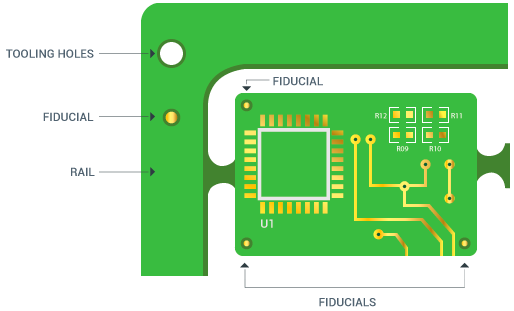
- Panelization: If producing multiple small LED PCBs, design them to fit on a larger panel for cost-effective manufacturing. Leave at least 2mm between individual boards for easy separation.
- Solder Mask and Finish: Use a white solder mask to reflect light and improve efficiency in lighting applications. A surface finish like ENIG (Electroless Nickel Immersion Gold) ensures good solderability for LED components.
- Testing: After assembly, test for thermal performance and electrical continuity. Use a thermal camera to check for hot spots that could indicate poor heat dissipation.
Conclusion: Building Better LED Lighting with Smart PCB Design
Designing a PCB for LED lighting applications requires a balance of size, performance, and thermal management. By understanding standard PCB dimensions for LED lighting, adhering to LED PCB design guidelines, prioritizing thermal management in LED PCBs, optimizing LED component placement, and addressing the unique needs of high-power LED PCB design, you can create reliable and efficient lighting solutions. Whether you're working on a small LED bulb or a large industrial fixture, these principles will guide you toward success.
At ALLPCB, we’re committed to supporting your design journey with high-quality manufacturing services tailored to your needs. Start applying these tips in your next project to achieve outstanding results in LED lighting design.
 ALLPCB


