ALLPCB


If you're struggling with solder paste printing on uneven surfaces, you're not alone. Applying solder paste to non-flat PCBs or non-planar surfaces can be a challenge, but with the right techniques and tools, it’s manageable. This guide offers practical solutions for solder paste uneven surfaces, including using stepped stencils, conformal coatings, and methods for filling gaps. Whether you're working on complex geometries or irregular boards, these tips will help you achieve reliable results.
In this detailed blog, we'll explore the unique challenges of solder paste non-planar surfaces, share actionable strategies, and provide insights into optimizing your process for consistent solder paste application. Let's dive into the world of non-flat PCBs and master the art of precision printing.
Understanding the Challenges of Solder Paste Printing on Uneven Surfaces
Printing solder paste on uneven or non-planar surfaces is far more complex than working with flat PCBs. Traditional stencil printing assumes a level surface, but when dealing with non-flat PCBs or components at varying heights, several issues arise. These include inconsistent paste deposition, insufficient contact between the stencil and board, and potential defects like bridging or insufficient solder volume.
For instance, on a board with raised components or a stepped design, the stencil may not sit flush, leading to gaps where paste doesn't transfer properly. This can result in weak solder joints or assembly failures. Understanding these challenges is the first step to overcoming them when working with solder paste uneven surfaces.
Why Non-Planar Surfaces Are Common in Modern PCB Designs
Modern electronics often require complex designs that go beyond flat, two-dimensional boards. Devices like wearables, medical implants, and automotive sensors frequently use non-planar surfaces or 3D molded interconnect devices (MIDs). These designs save space and improve functionality but complicate the assembly process, especially during solder paste application.
For example, a wearable fitness tracker might have a curved PCB to fit snugly against the wrist. Applying solder paste on non-planar surfaces like this requires specialized techniques to ensure even distribution and reliable connections. As these designs become more common, mastering techniques for uneven surfaces is essential for manufacturers and hobbyists alike.
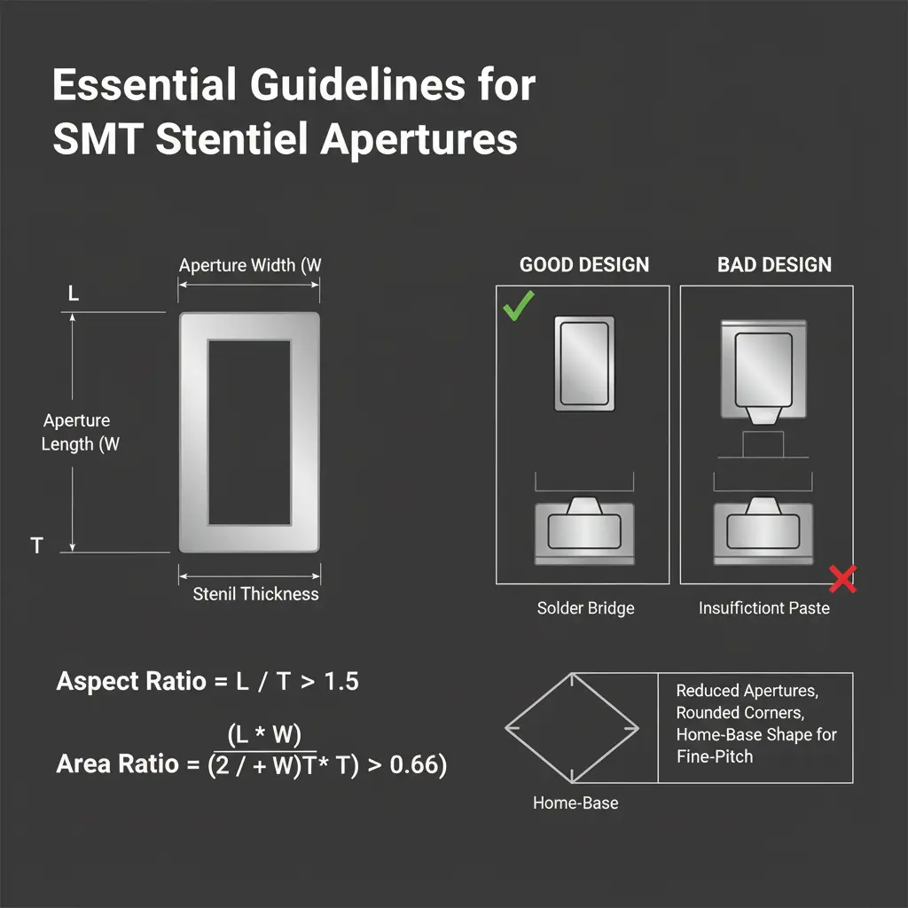
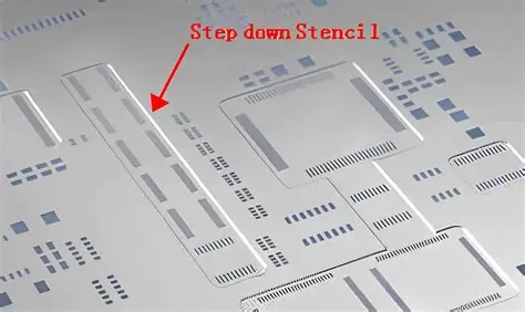
Tip 1: Use Stepped Stencils for Solder Paste on Uneven Surfaces
One of the most effective solutions for solder paste stepped stencils is using a custom-designed stencil with varying thicknesses. Stepped stencils are engineered to accommodate height differences on a PCB, allowing for precise paste application across uneven areas.
Here’s how they work: The stencil is thicker in areas where the PCB is lower and thinner where components or board sections are raised. This ensures the stencil contacts all areas of the board evenly during printing. For instance, if a board has a section raised by 0.5 mm due to a mounted component, a stepped stencil can be designed with a corresponding step-down to maintain contact.
When ordering or designing a stepped stencil, ensure the step height matches the PCB's topography. Also, use a high-quality stencil material like stainless steel for durability and precision. This method is particularly useful for non-flat PCBs with consistent height variations.
Tip 2: Optimize Squeegee Pressure and Angle for Non-Planar Surfaces
When printing solder paste on non-planar surfaces, adjusting the squeegee pressure and angle can make a significant difference. On a flat board, standard settings (like a 60-degree angle and moderate pressure) work well. However, uneven surfaces require fine-tuning to ensure even paste distribution.
Start by reducing squeegee pressure slightly to avoid forcing paste through gaps or creating uneven deposits. A pressure range of 3-5 kg is often a good starting point for manual or semi-automated systems, though this varies by equipment. Additionally, experiment with a slightly shallower angle (around 45 degrees) to improve contact on raised or lowered areas.
Consistency is key. Test your settings on a sample board and inspect the paste deposit for uniformity. If you notice thin or missing paste in certain areas, adjust incrementally until the results are satisfactory. This approach helps tackle challenges with solder paste uneven surfaces.
Tip 3: Leverage Conformal Coating for Solder Paste Application
Another strategy for managing solder paste conformal coating involves using a protective layer to smooth out uneven surfaces before printing. Conformal coatings are typically used to protect PCBs from environmental factors, but they can also help create a more uniform surface for solder paste application.
For example, if a PCB has minor height variations (less than 0.2 mm), applying a thin conformal coating can fill small gaps and create a flatter surface. After the coating cures, the stencil can make better contact, improving paste transfer. Be cautious, though—coatings add an extra step and may not be suitable for all designs, especially if thermal or electrical properties are affected.
Choose a coating compatible with your solder paste and reflow process. Acrylic or silicone-based coatings are common options, offering flexibility and ease of application. This method is a creative workaround for non-flat PCBs with subtle irregularities.
Tip 4: Fill Gaps with Solder Paste for Seamless Connections
When dealing with solder paste filling gaps, a targeted approach can prevent voids and ensure strong solder joints. Uneven surfaces often create small gaps between the stencil and PCB, leading to insufficient paste in critical areas. Manually or mechanically filling these gaps after initial printing can solve this issue.
Use a small syringe or dispensing tool to apply additional solder paste into areas where deposition is thin. For precision, opt for a needle tip with a diameter of 0.4 mm or smaller to control the paste volume. After filling, inspect the board to ensure no excess paste causes bridging during reflow.
This technique is especially useful for prototypes or small-batch production where custom stencils may not be cost-effective. It’s a hands-on solution for managing solder paste uneven surfaces without investing in specialized equipment.
Tip 5: Consider Jet Printing for Complex Non-Planar Surfaces
For highly irregular or solder paste non-planar surfaces, traditional stencil printing may not be feasible. In such cases, jet printing offers a flexible alternative. Jet printers deposit solder paste directly onto the PCB using a nozzle, eliminating the need for a stencil and allowing precise application on uneven or curved surfaces.
Jet printing systems can adjust paste volume dynamically, depositing more in recessed areas and less on raised sections. This adaptability makes them ideal for 3D MIDs or boards with extreme height variations (e.g., differences of 1 mm or more). While jet printing equipment is more expensive than stencil systems, it’s a worthwhile investment for high-complexity projects.
If you’re working on a design with significant topographical challenges, explore jet printing as a solution for non-flat PCBs. Many modern assembly houses offer this service, saving you the upfront cost of equipment.
Tip 6: Use 3D Toolpaths for Custom Printing on Uneven Surfaces
Inspired by advancements in additive manufacturing, adapting 3D toolpaths for solder paste application is an innovative approach for solder paste uneven surfaces. This method involves programming a dispensing system to follow the contours of a non-planar PCB, ensuring paste is applied evenly across all areas.
For instance, if a board curves upward by 2 mm over a 10 cm span, a 3D toolpath can guide the dispenser along this curve, maintaining a consistent distance from the surface. Software for generating such toolpaths is often available with advanced dispensing systems, and some open-source options can be adapted for custom setups.
This technique requires precise calibration and mapping of the PCB’s surface, often using a 3D scanner or manual measurements. It’s a cutting-edge solution for solder paste non-planar surfaces, particularly in research or niche applications.
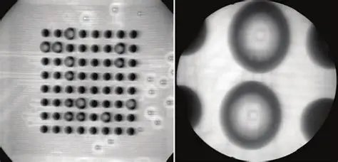
Tip 7: Inspect and Adjust After Printing
Regardless of the method used, inspection is critical when working with non-flat PCBs. After applying solder paste, use a magnifying glass or automated optical inspection (AOI) system to check for inconsistencies. Look for areas with too little paste (which can cause open circuits) or too much paste (which can lead to bridging).
If issues are found, make adjustments before reflow. For small corrections, manually add or remove paste with a fine tool. For systemic problems, revisit your stencil design, squeegee settings, or printing method. A typical target for paste height is 0.1 to 0.15 mm for most surface-mount components, though this varies by design.
Regular inspection ensures high-quality results, especially when dealing with the unpredictability of solder paste uneven surfaces.
Common Pitfalls to Avoid with Solder Paste on Non-Planar Surfaces
Even with the best techniques, mistakes can happen. Here are a few pitfalls to watch out for when printing solder paste on non-planar surfaces:
- Overloading Paste: Applying too much paste to compensate for unevenness can cause shorts during reflow. Stick to recommended volumes (e.g., 0.5 to 0.8 mm3 per pad for small components).
- Ignoring Stencil Alignment: Misalignment between the stencil and PCB, especially on stepped designs, can ruin paste distribution. Double-check alignment before printing.
- Skipping Tests: Always run a test print on a scrap board to fine-tune settings before full production. This saves time and materials when working with non-flat PCBs.
Conclusion: Mastering Solder Paste Printing on Uneven Surfaces
Applying solder paste on uneven surfaces doesn’t have to be a daunting task. By using tools like solder paste stepped stencils, optimizing squeegee settings, exploring solder paste conformal coating, and leveraging advanced methods like jet printing or 3D toolpaths, you can achieve consistent and reliable results. Techniques for solder paste filling gaps and thorough post-printing inspections further ensure success, even on the most challenging non-flat PCBs.
Whether you're an engineer tackling a complex design or a hobbyist experimenting with innovative layouts, these tips and tricks for solder paste non-planar surfaces will help you overcome obstacles and improve your assembly process. With practice and the right approach, uneven surfaces become just another solvable challenge in PCB manufacturing.