 ALLPCB


In the world of electronics design, maintaining signal integrity in small printed circuit boards (PCBs) is a growing challenge. As devices become more compact and high-speed circuits become the norm, engineers often face issues like signal reflection, impedance mismatches, and crosstalk. So, how do you ensure signal integrity in small PCBs? The key lies in understanding the unique constraints of compact designs and applying best practices for impedance control, routing, and noise reduction.
In this comprehensive guide, we’ll dive deep into the specific signal integrity issues in small PCBs, explore the impact of PCB size on signal integrity, and provide actionable solutions for high-speed PCB design. Whether you’re designing for IoT devices, wearables, or other compact systems, this blog will equip you with the knowledge to tackle these challenges head-on.
What Is Signal Integrity and Why Does It Matter in Small PCBs?
Signal integrity refers to the quality of an electrical signal as it travels through a PCB. A signal with good integrity remains clear and undistorted, ensuring that data is transmitted accurately. In small PCBs, maintaining this quality is tougher due to limited space, tighter trace layouts, and the need for high-speed performance in applications like 5G, USB, or DDR memory interfaces.
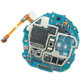
Small PCBs, often under 50 mm x 50 mm in size, are common in modern devices such as smartwatches, wireless earbuds, and medical sensors. However, their compact nature amplifies signal integrity issues. Traces are closer together, increasing the risk of interference, while limited space for components like decoupling capacitors can lead to power delivery problems. Addressing these challenges is critical to prevent data errors, system crashes, or performance degradation.
Key Signal Integrity Issues in Small PCBs
Designing small PCBs for high-speed applications comes with a unique set of hurdles. Let’s break down the most common signal integrity issues and why they are particularly problematic in compact designs.
1. Signal Reflection Due to Impedance Mismatches
Signal reflection occurs when a signal encounters a change in impedance along its path, causing part of the signal to bounce back. In small PCBs, achieving consistent impedance is challenging because trace lengths are short, and there’s little room for proper termination components like resistors. For high-speed signals operating at frequencies above 1 GHz, even a small mismatch can cause reflections that distort the signal waveform.
For example, a typical 50-ohm impedance requirement for high-speed USB lines can be disrupted by abrupt changes in trace width or layer transitions, which are hard to avoid in a cramped layout. Reflections can lead to data errors, especially in protocols requiring precise timing.
2. Crosstalk in Tight Layouts
Crosstalk happens when signals on adjacent traces interfere with each other, creating noise. In small PCBs, traces are often packed closely together, sometimes with spacing as tight as 0.1 mm. At high frequencies, such as those used in DDR4 memory (up to 3.2 GHz), this proximity increases electromagnetic coupling, degrading signal quality.
The smaller the board, the harder it is to maintain adequate spacing or add ground planes between traces to act as shields. This makes crosstalk a significant concern for engineers working on compact designs.
3. Power Integrity and Limited Decoupling
Power integrity is closely tied to signal integrity. Voltage fluctuations on power lines can introduce noise into signals, especially in high-speed circuits. Small PCBs often lack space for enough decoupling capacitors near ICs, which are essential for stabilizing voltage. Without proper decoupling, a sudden current demand from a high-speed processor can cause a voltage drop, leading to signal errors.
For instance, in a small IoT module with a microcontroller running at 100 MHz, insufficient decoupling might result in jitter, affecting communication reliability over protocols like I2C or SPI.
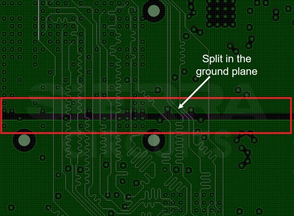
4. Limited Ground Plane Area
A solid ground plane is vital for providing a low-impedance return path for signals and reducing electromagnetic interference (EMI). In small PCBs, there’s often not enough room for a continuous ground plane, especially in multi-layer designs where space is split between signal and power layers. Fragmented ground planes can lead to higher loop inductance, worsening signal integrity at frequencies above 500 MHz.
Impact of PCB Size on Signal Integrity
The relationship between PCB size and signal integrity is direct and significant. Smaller boards impose physical constraints that make traditional signal integrity solutions harder to implement. Here are some specific ways PCB size impacts signal quality:
- Reduced Trace Spacing: As board size shrinks, traces must be placed closer together, increasing the risk of crosstalk. For high-speed designs, maintaining a spacing-to-height ratio of at least 3:1 (trace spacing to dielectric height) is ideal, but this is often unfeasible in small PCBs.
- Shorter Trace Lengths: While shorter traces reduce signal delay, they can complicate impedance matching. High-speed signals may require precise trace lengths for timing, which is difficult to achieve in a confined space.
- Component Density: High component density in small PCBs leaves little room for vias, ground pours, or shielding, all of which are crucial for minimizing noise and interference.
Understanding these constraints is the first step to designing effective solutions tailored to compact boards. The smaller the PCB, the more creative and precise your approach needs to be.
Solutions for Signal Integrity in Small PCBs
While the challenges are significant, there are proven strategies to maintain signal integrity in small PCBs, even for high-speed designs. Below are actionable solutions focusing on impedance control, routing, and noise reduction.
1. Prioritize Impedance Control
Impedance control is the foundation of good signal integrity. For small PCBs, achieving a consistent impedance (often 50 ohms for high-speed signals) requires careful planning:
- Use Controlled Dielectric Materials: Choose PCB materials with a stable dielectric constant (Dk), such as FR-4 with a Dk of around 4.2, to ensure predictable impedance. For very high frequencies, consider low-loss materials like Rogers laminates.
- Calculate Trace Widths: Use impedance calculators to determine the correct trace width for your target impedance. For a 50-ohm microstrip on a 1.6 mm FR-4 board, a trace width of about 0.3 mm is typical, though this varies with stack-up.
- Minimize Vias: Vias introduce impedance discontinuities. When unavoidable, use back-drilling or blind vias to reduce stub effects in high-speed designs above 5 GHz.
2. Optimize Routing for High-Speed PCB Design
Routing is critical in small PCBs where every millimeter counts. Follow these best practices to reduce signal reflection and crosstalk:
- Keep Traces Short and Direct: Minimize trace length to reduce signal delay and potential for reflection. For differential pairs like USB or Ethernet, match trace lengths within 0.1 mm to avoid skew.
- Avoid Sharp Corners: Use 45-degree bends or curved traces instead of 90-degree angles to prevent signal reflection at high frequencies.
- Separate High-Speed Signals: Route high-speed traces away from noise sources like switching regulators. If space is tight, use guard traces connected to ground to isolate sensitive lines.
3. Enhance Power Integrity
Stable power delivery is essential for signal quality. In small PCBs, focus on these techniques:
- Place Decoupling Capacitors Close to ICs: Use small-value capacitors (e.g., 0.1 μF) near power pins to filter high-frequency noise. If space is limited, consider embedded capacitance in the PCB stack-up.
- Use Power Planes: Even in small designs, dedicate a layer or section to a power plane to ensure low-impedance power distribution. Split planes if different voltage levels are needed, but avoid routing signals over splits.
4. Maximize Ground Plane Effectiveness
Even with limited space, a well-designed ground plane can significantly improve signal integrity:
- Create a Continuous Ground Layer: If possible, dedicate an entire layer to ground in a 4-layer or higher stack-up. For 2-layer boards, maximize ground pour on both sides and stitch with vias.
- Reduce Return Path Loops: Ensure signal return paths are short by placing ground vias near signal vias. This reduces loop inductance, critical for signals above 1 GHz.
5. Simulate and Test Designs
Before manufacturing, use simulation tools to identify potential signal integrity issues. Software can model impedance, crosstalk, and reflections for high-speed PCB design. Post-manufacturing, test your board with an oscilloscope to measure signal rise times and eye diagrams. For example, a clean eye diagram for a 2.5 Gbps signal should show minimal jitter and clear openings, indicating good integrity.
Advanced Considerations for High-Speed Small PCBs
For engineers pushing the limits with frequencies above 10 GHz, such as in 5G modules or advanced IoT devices, additional measures are necessary:
- Differential Signaling: Use differential pairs for high-speed data to cancel out noise. Maintain tight length matching (within 0.05 mm) and consistent spacing for pairs.
- Advanced Materials: Opt for low-loss dielectrics with Dk values below 3.5 to minimize signal attenuation in compact designs.
- EMI Shielding: Incorporate metal cans or conductive gaskets around sensitive areas if board space allows, to block external interference.
Conclusion: Mastering Signal Integrity in Small PCBs
Designing small PCBs for high-speed applications presents unique signal integrity challenges, from signal reflection and impedance mismatches to crosstalk and power noise. However, with careful planning and the right strategies, these issues can be managed effectively. Focus on impedance control, optimized routing, robust power delivery, and solid grounding to ensure reliable performance, even in the tightest layouts.
By understanding the impact of PCB size on signal integrity and applying the solutions outlined in this guide, engineers can create compact, high-speed designs that meet the demands of modern electronics. Whether you’re working on a tiny wearable or a complex IoT module, mastering signal integrity is the key to success in small PCB design.


