ALLPCB


In the world of electronics manufacturing, the quality and reliability of a printed circuit board (PCB) are critical to the performance of the final product. One of the most important aspects of ensuring this quality lies in inspecting the inner layers of multilayer PCBs. But what are the best techniques for PCB inner layer inspection? At the core, methods like Automated Optical Inspection (AOI), X-ray inspection, and microsection analysis stand out as powerful tools to detect defects and ensure reliability. In this comprehensive guide, we’ll dive deep into these techniques—focusing on PCB inner layer AOI, X-ray inspection for inner layers, and microsection analysis for inner layers—to help engineers and manufacturers understand how to maintain the highest standards in PCB production.
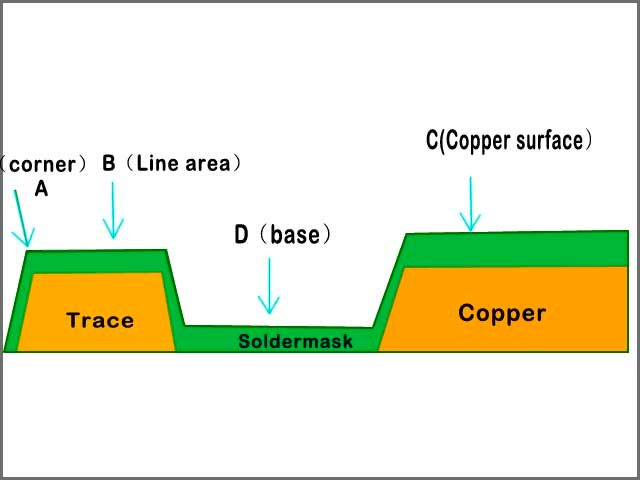
Why Inner Layer Inspection Matters in PCB Manufacturing
Multilayer PCBs are the backbone of modern electronics, used in everything from smartphones to medical devices. These boards consist of multiple layers of conductive material, often copper, sandwiched between insulating layers. The inner layers are hidden from view, making it challenging to spot defects like misalignments, shorts, or incomplete etching. If left undetected, these issues can lead to signal integrity problems, impedance mismatches, or even complete board failure. For instance, a misalignment in an inner layer could disrupt a high-speed signal path, reducing data transfer rates by as much as 20% in critical applications.
Inner layer inspection is essential to catch these flaws early in the manufacturing process. By using advanced techniques, manufacturers can ensure that each layer meets strict quality standards, maintaining signal integrity (often targeting impedance values within ±10% of design specs, such as 50 ohms for high-speed signals) and preventing costly rework or product recalls. Let’s explore the three primary methods for inspecting PCB inner layers and how they contribute to quality and reliability.
1. PCB Inner Layer AOI: Precision Through Automated Optical Inspection
Automated Optical Inspection (AOI) is a widely used technique for inspecting both outer and inner layers of PCBs during manufacturing. For inner layers, AOI systems use high-resolution cameras and advanced software algorithms to scan the surface of each layer before they are laminated together. This non-destructive method is ideal for detecting surface-level defects such as scratches, incomplete copper traces, or over-etching.
How PCB Inner Layer AOI Works
During the AOI process, the inner layer is placed under a specialized camera system that captures detailed images of the copper patterns. These images are compared against the original design files (often Gerber files) to identify discrepancies. Modern AOI systems can detect defects as small as 10 micrometers, ensuring that even the tiniest flaws are caught before the layers are stacked and laminated. For example, if a trace width deviates by more than 5% from the intended 0.2 mm, the system flags it for review.
Advantages of PCB Inner Layer AOI
- Speed: AOI systems can inspect an entire layer in minutes, making them ideal for high-volume production.
- Accuracy: With resolutions down to micrometer levels, AOI ensures precise defect detection.
- Non-Destructive: Since AOI relies on optical imaging, it doesn’t damage the PCB during inspection.
Limitations of AOI for Inner Layers
While AOI is highly effective for surface defects, it cannot inspect the internal structure of a layer or detect issues like delamination or voids beneath the surface. Once the layers are laminated, AOI is no longer an option for inner layer inspection. This is where other techniques, like X-ray inspection, come into play.
2. X-Ray Inspection for Inner Layers: Seeing Beneath the Surface
X-ray inspection for inner layers is a powerful non-destructive testing method that allows manufacturers to peer inside a fully assembled multilayer PCB. This technique is particularly valuable for detecting hidden defects that AOI cannot identify, such as misregistration between layers, internal voids, or issues with vias and through-holes.
How X-Ray Inspection for Inner Layers Works
X-ray inspection systems use high-energy X-rays to penetrate the PCB and create detailed images of its internal structure. These systems can generate 2D or even 3D images, revealing the alignment of inner layers and the integrity of connections like blind or buried vias. For instance, in a 12-layer PCB, X-ray inspection can confirm that all layers are aligned within a tolerance of ±0.05 mm, ensuring proper signal transmission at speeds up to 10 Gbps.
Advanced X-ray systems often incorporate AI-powered imaging to enhance defect detection. These systems can identify issues like insufficient copper plating in vias, which could lead to a 15% increase in electrical resistance, compromising the board’s performance.
Benefits of X-Ray Inspection for Inner Layers
- Non-Destructive: X-ray inspection allows for thorough testing without damaging the PCB.
- Comprehensive: It reveals hidden defects in inner layers, vias, and solder joints that are invisible to optical methods.
- Precision: Modern systems offer resolution down to 1 micrometer, ideal for high-density interconnect (HDI) boards.
Challenges of X-Ray Inspection
While X-ray inspection is highly effective, it requires specialized equipment and trained operators, which can increase costs. Additionally, interpreting X-ray images can be complex, especially for densely packed multilayer boards with overlapping features. However, advancements in imaging software are making this process faster and more accessible.
3. Microsection Analysis for Inner Layers: A Detailed Destructive Approach
Microsection analysis for inner layers, also known as cross-sectioning, is a destructive testing method that provides an in-depth look at the internal structure of a PCB. While it cannot be used on every board due to its destructive nature, it is invaluable for quality control sampling and failure analysis.
How Microsection Analysis for Inner Layers Works
In microsection analysis, a small sample of the PCB is cut, mounted in resin, and polished to create a cross-sectional view. This sample is then examined under a high-powered microscope to inspect the inner layers, vias, and dielectric materials. For example, manufacturers might check the thickness of the copper plating in a via, ensuring it meets a minimum of 25 micrometers as per industry standards like IPC-6012. They can also measure the dielectric spacing between layers, targeting values like 0.1 mm to prevent crosstalk in high-frequency designs.
Advantages of Microsection Analysis
- Highly Detailed: It provides a clear view of internal structures, revealing issues like delamination or plating defects.
- Accurate Measurements: Microscopes can measure features with sub-micrometer precision, ensuring compliance with design specs.
- Root Cause Analysis: It’s ideal for investigating failures, such as identifying why a via failed under thermal stress.
Limitations of Microsection Analysis
The primary drawback of microsection analysis is that it destroys the tested sample, making it unsuitable for inspecting every board. It’s typically used on a small percentage of production batches or during failure investigations. Additionally, the process is time-consuming, often taking several hours per sample.
Comparing PCB Inner Layer Inspection Techniques
Each of these inspection methods—PCB inner layer AOI, X-ray inspection for inner layers, and microsection analysis for inner layers—has its strengths and weaknesses. Choosing the right technique depends on the stage of production, the type of PCB, and the specific quality requirements.
- AOI is best for pre-lamination inspection of inner layers, focusing on surface defects with speed and precision.
- X-Ray Inspection excels at post-lamination testing, revealing hidden flaws without damaging the board.
- Microsection Analysis offers unparalleled detail for quality sampling and failure analysis, despite being destructive.
For high-reliability applications, such as aerospace or medical devices, a combination of all three methods is often used. For instance, AOI can ensure surface quality before lamination, X-ray inspection can verify alignment and internal connections after assembly, and microsection analysis can validate material integrity on a sample basis.
Best Practices for Ensuring PCB Inner Layer Quality
To achieve the highest levels of quality and reliability in PCB manufacturing, consider these best practices for inner layer inspection:
- Integrate Multiple Techniques: Use AOI for early-stage checks, X-ray for assembled boards, and microsection analysis for periodic validation.
- Adhere to Standards: Follow industry standards like IPC-A-600 for acceptability criteria, ensuring inner layer features meet tolerances (e.g., trace spacing within ±0.02 mm).
- Invest in Technology: Utilize the latest inspection equipment with high resolution and AI capabilities to improve defect detection rates by up to 30%.
- Train Personnel: Ensure that operators are skilled in interpreting inspection data, especially for complex X-ray images or microsection samples.
The Role of Inner Layer Inspection in High-Density Interconnect (HDI) PCBs
As electronics become smaller and more complex, HDI PCBs with finer traces (as narrow as 0.075 mm) and microvias (diameters below 0.15 mm) are increasingly common. These boards demand even stricter inner layer inspection due to their tight tolerances. X-ray inspection is particularly critical for verifying microvia alignment and plating quality, while microsection analysis helps confirm dielectric thickness, often targeting values as low as 0.05 mm to prevent signal interference.
Without proper inspection, defects in HDI PCBs can lead to significant performance issues, such as a 25% reduction in signal speed or increased noise in high-frequency applications. By prioritizing inner layer inspection, manufacturers can ensure that HDI boards meet the demands of cutting-edge technologies.
Conclusion: Building Reliability Through Inner Layer Inspection
The quality and reliability of a PCB hinge on the integrity of its inner layers, which are often the most challenging to inspect. Techniques like PCB inner layer AOI, X-ray inspection for inner layers, and microsection analysis for inner layers provide manufacturers with the tools needed to detect and address defects at every stage of production. By leveraging these methods, engineers can ensure that their boards meet stringent performance requirements, whether it’s maintaining impedance within ±5% of a 50-ohm target or ensuring signal speeds of 5 Gbps or higher.
At ALLPCB, we are committed to delivering the highest standards in PCB manufacturing by integrating advanced inspection techniques into our processes. Whether you’re designing a simple two-layer board or a complex HDI PCB, understanding and applying these inner layer inspection methods is key to achieving flawless results. With the right approach, you can build electronics that are not only functional but also reliable for years to come.