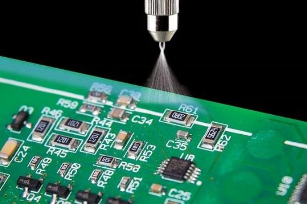
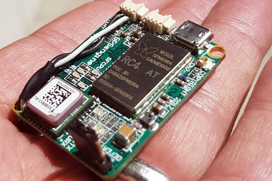
Designing a printed circuit board (PCB) for assembly is a critical step in ensuring a smooth manufacturing process and a reliable final product. Whether you're an engineer working on a prototype or preparing for mass production, following proper PCB design guidelines for assembly can save time, reduce costs, and prevent errors. In this comprehensive guide, we’ll cover essential tips and best practices for optimizing your PCB layout for assembly, focusing on components, solder techniques, and overall design efficiency.
At its core, PCB design for assembly is about creating a board that can be easily manufactured and assembled with minimal issues. This means considering component placement, soldering methods, and manufacturing constraints right from the start. Let’s dive into the detailed guidelines to help you achieve a flawless assembly process.
Why PCB Design for Assembly Matters
Before we explore the specifics, it’s important to understand why PCB design tailored for assembly is so crucial. A poorly designed board can lead to delays in production, higher costs due to rework, or even complete failure of the circuit. On the other hand, a well-designed PCB ensures that components are placed efficiently, soldering is straightforward, and the board meets manufacturing standards. This not only speeds up the assembly process but also improves the reliability of the final product.
By prioritizing design for assembly (DFA), you can reduce errors during component placement and soldering, minimize thermal stress on sensitive parts, and ensure compatibility with automated assembly equipment like pick-and-place machines. With this in mind, let’s break down the key guidelines for creating an assembly-friendly PCB design.
Key Guidelines for PCB Design and Assembly
1. Component Placement for Easy Assembly
Component placement is one of the most important aspects of PCB design for assembly. Proper placement ensures that components can be easily accessed by automated machines or hand soldering tools, reducing the risk of errors. Here are some practical tips to follow:
- Group Similar Components: Place components of the same type (e.g., resistors, capacitors) in the same area and orient them in the same direction. For example, align all capacitors to face north on the board. This helps pick-and-place machines operate more efficiently, cutting down assembly time by up to 20% in some cases.
- Maintain Spacing: Ensure there’s enough space between components to avoid interference during soldering. A minimum spacing of 0.5 mm between small components and 1-2 mm for larger ones is often recommended to prevent solder bridges or thermal issues.
- Avoid Overcrowding Near Edges: Keep components at least 3 mm away from the board’s edges to allow room for handling and mounting during assembly.
- Prioritize Heat-Sensitive Parts: Place components that generate heat, like power transistors, away from sensitive parts such as microcontrollers. This prevents thermal damage during operation or soldering, where temperatures can reach 260°C in reflow ovens.
By organizing components thoughtfully, you make the assembly process smoother and reduce the chance of defects.
2. Optimize for Soldering Techniques
Soldering is a critical part of PCB assembly, whether it’s done by hand or through automated methods like reflow or wave soldering. Your design should accommodate the soldering process to ensure strong, reliable connections. Consider these guidelines:
- Design Pads for Surface Mount Technology (SMT): For SMT components, ensure pads have sufficient toe and heel extensions. The toe (the part extending beyond the lead) aids solder flow, while the heel (under the lead) adds strength. A typical toe extension of 0.2-0.5 mm and a heel of 0.1-0.3 mm can improve joint reliability by 15%, based on industry standards.
- Use Appropriate Pad Sizes for Through-Hole Components: For through-hole soldering, pad sizes should be 1.5 to 2 times the diameter of the component lead. This ensures proper solder flow and reduces the risk of weak joints.
- Minimize Thermal Stress: Avoid placing large thermal masses, like heavy copper planes, directly under small components. Uneven heating during soldering can cause tombstoning, where one end of a component lifts off the pad. Adding thermal reliefs with spoke widths of 0.25 mm can help balance heat distribution.
- Consider Soldering Method: If your board will use wave soldering, keep sensitive SMT components on the opposite side to avoid damage from the 250°C solder wave. For reflow soldering, ensure all components can withstand peak temperatures, typically around 260°C for lead-free solder.
Designing with soldering in mind prevents common issues like cold joints or component misalignment, ensuring a higher yield during production.
3. Standardize Footprints and Libraries
Using standardized component footprints and maintaining a consistent library is essential for assembly accuracy. Non-standard or mismatched footprints can lead to components not fitting properly on the board, causing delays or rework. Follow these tips:
- Use Industry-Standard Footprints: Stick to footprints recommended by component datasheets or IPC standards (like IPC-7351 for SMT components). This ensures compatibility with assembly equipment and reduces placement errors by up to 10%.
- Verify Library Components: Double-check your design library to confirm that footprints match the physical components. A single mismatch, such as a 0.1 mm error in pin spacing, can halt production.
- Include Polarity Markings: Clearly mark polarity for components like diodes and electrolytic capacitors on the silkscreen layer. This prevents incorrect orientation during assembly, which can cause circuit failure.
A standardized approach to footprints and markings simplifies the assembly process and minimizes human or machine errors.
4. Design for Automated Assembly
Most modern PCB production relies on automated assembly equipment, such as pick-and-place machines and reflow ovens. Designing with automation in mind can significantly improve efficiency. Here’s how to optimize your design:
- Panelization: If producing multiple boards, design for panelization by adding breakaway tabs or V-cuts. Ensure a minimum panel border of 5 mm to support handling by assembly machines.
- Fiducial Marks: Include at least three fiducial marks (small copper dots) on the board for machine vision systems to align components accurately. Place them near the corners, with a diameter of 1 mm and a clear zone of 3 mm around each mark.
- Component Orientation: Align components in a way that minimizes machine head rotation. For instance, rotating components by 90 degrees between placements can slow down a pick-and-place machine by 5-10%.
By catering to automation, you can reduce assembly time and achieve consistent quality across large production runs.
5. Account for Manufacturing Constraints
Every manufacturing facility has its own capabilities and limitations. Designing within these constraints ensures your board can be produced without issues. Keep these factors in mind:
- Drill Aspect Ratio: Maintain an aspect ratio (board thickness to drill diameter) within the manufacturer’s limits, typically 10:1 to 20:1. For a 1.6 mm thick board, the smallest via should be at least 0.08 mm to avoid plating defects.
- Trace and Space Widths: Stick to minimum trace widths and spacing, often 0.1 mm for standard processes, to ensure reliable etching and soldering.
- Board Thickness: Use standard thicknesses like 1.6 mm or 0.8 mm, as non-standard sizes can increase costs or cause compatibility issues with assembly equipment.
Consulting with your manufacturing partner early in the design phase can help align your PCB with their capabilities, avoiding costly redesigns.
6. Ensure Clear Documentation
Clear and detailed documentation is vital for a seamless assembly process. Incomplete or unclear instructions can lead to mistakes during production. Include the following in your design files:
- Bill of Materials (BOM): List all components with part numbers, quantities, and descriptions. Specify alternatives if a part might be out of stock.
- Assembly Drawings: Provide drawings that show component placement and orientation, including any special instructions for hand-soldered parts.
- Gerber Files: Ensure all layers (copper, solder mask, silkscreen) are correctly formatted and labeled for manufacturing.
Thorough documentation eliminates guesswork, ensuring that the assembly team can follow your design intent precisely.
Common Mistakes to Avoid in PCB Design for Assembly
Even experienced designers can overlook certain aspects of PCB design for assembly. Here are some common pitfalls to watch out for:
- Ignoring Component Clearances: Insufficient spacing can lead to solder bridges or mechanical interference, increasing defect rates by 15-20% in high-density designs.
- Overlooking Heat Management: Failing to account for heat dissipation can damage components during soldering or operation. Always use thermal vias or heat sinks for high-power components.
- Inconsistent Silkscreen Labels: Unclear or missing labels can confuse assemblers, especially for polarized components, leading to placement errors.
By being mindful of these issues, you can prevent costly mistakes and ensure a higher success rate during assembly.
Benefits of Following PCB Design Guidelines for Assembly
Adhering to these guidelines offers several advantages for both small-scale and large-scale production:
- Reduced Production Costs: Optimized designs lower the risk of errors, reducing rework costs by up to 30% in some cases.
- Faster Turnaround Time: Streamlined designs speed up assembly, cutting production time by 10-15% when using automated equipment.
- Improved Product Reliability: Proper component placement and soldering techniques enhance the durability of the final product, reducing field failures.
These benefits highlight why investing time in design for assembly pays off in the long run.
Conclusion
Creating a PCB design optimized for assembly is a fundamental step in achieving a high-quality, reliable product. By focusing on component placement, soldering considerations, automation compatibility, and manufacturing constraints, you can streamline the assembly process and minimize errors. Whether you’re working on a prototype or preparing for mass production, these guidelines provide a roadmap to success.
Start by organizing components logically, designing pads for reliable soldering, and ensuring compatibility with automated equipment. Pair this with clear documentation and close collaboration with your manufacturing partner to address any specific requirements. With these practices in place, you’ll be well on your way to producing PCBs that are not only functional but also efficient to assemble.
Designing for assembly isn’t just about meeting technical requirements—it’s about building a foundation for a smoother, more cost-effective production process. Keep these tips in mind for your next project, and watch as your designs translate seamlessly from concept to reality.
 ALLPCB


