Designing a printed circuit board (PCB) for electromagnetic compatibility (EMC) is crucial to ensure your electronic devices function without interference and meet regulatory standards. If you're wondering how to achieve EMC in PCB design, the answer lies in using the right diagnostic tools and techniques like near field scanning, spectrum analyzers, and proper PCB layout strategies. In this blog, we'll dive deep into the essentials of PCB EMC, exploring tools and methods to diagnose and mitigate electromagnetic interference (EMI), along with practical tips for signal integrity, EMI shielding, PCB grounding, and layout optimization.
Why EMC Matters in PCB Design
Electromagnetic compatibility, or EMC, is the ability of an electronic device to operate in its environment without causing or being affected by electromagnetic interference. Poor EMC design can lead to signal disruptions, data loss, or failure to pass regulatory tests, which can delay product launches and increase costs. For engineers, ensuring EMC starts at the PCB level, where layout, grounding, and shielding play pivotal roles.
EMC issues often stem from high-frequency signals, improper grounding, or inadequate spacing between traces. By addressing these during the design phase and using diagnostic tools to identify problems, you can save time and resources. Let's explore the key aspects of PCB design for EMC and the tools that help achieve it.
Key Elements of PCB Design for EMC
Before diving into diagnostic tools, it's important to understand the core principles of designing a PCB for EMC. These include signal integrity, PCB grounding, EMI shielding, and layout optimization. Let's break these down.
1. Signal Integrity for Reduced Interference
Signal integrity refers to maintaining the quality of electrical signals as they travel through the PCB. Poor signal integrity can cause EMI, leading to EMC failures. To optimize signal integrity, keep high-speed signal traces as short as possible and avoid routing them near noisy components. For example, a signal operating at 1 GHz requires controlled impedance, often around 50 ohms, to prevent reflections and crosstalk.
Use differential pairs for high-speed signals and ensure consistent trace width to maintain impedance. Also, avoid sharp corners in traces, as they can act as antennas, radiating EMI. A 45-degree angle or curved trace is a better choice for high-frequency signals.
2. PCB Grounding Techniques
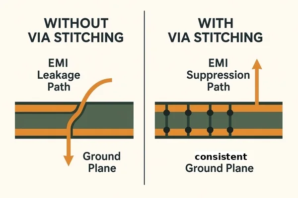
Effective grounding is one of the most critical factors in achieving EMC. A solid ground plane reduces noise by providing a low-impedance path for return currents. For multilayer PCBs, dedicate an entire layer to grounding to minimize loop areas that can emit or pick up interference.
For two-layer boards, create a ground grid beneath signal traces to mimic a ground plane's effect. Split ground planes should be avoided unless necessary for analog and digital separation, as they can create EMI issues. When splitting is required, ensure a single connection point to prevent ground loops.
3. EMI Shielding Strategies
EMI shielding involves blocking electromagnetic fields from interfering with or escaping the PCB. Place sensitive components away from high-noise areas and use metal enclosures or cans over critical sections. Additionally, incorporate decoupling capacitors near power pins of ICs to filter high-frequency noise. A typical value for decoupling capacitors is 0.1 μF, paired with a larger 10 μF capacitor for bulk filtering.
4. PCB Layout Best Practices
A well-thought-out PCB layout is the foundation of EMC. Group components by function, separating analog and digital sections to prevent crosstalk. Keep power and ground traces wide to handle current without voltage drops. For high-speed designs, maintain a trace spacing of at least three times the trace width to reduce coupling between adjacent lines.
Route critical signals first, ensuring they have the shortest and most direct paths. Avoid running signal traces over splits in the ground plane, as this increases the loop area and EMI risk. These layout practices set the stage for effective EMC before diagnostic tools come into play.
Diagnostic Tools for PCB EMC
Even with the best design practices, EMC issues can arise due to unforeseen factors like component placement or manufacturing variations. Diagnostic tools help identify and resolve these issues. Below are the most effective tools and techniques for diagnosing EMC problems in PCB design.
1. Near Field Scanning for EMI Detection
Near field scanning is a powerful technique for locating EMI sources on a PCB. It uses a small probe to measure electromagnetic fields close to the board's surface, typically within a few millimeters. This method helps pinpoint areas where EMI is radiating, such as near high-speed traces or poorly grounded components.
Near field probes come in electric (E-field) and magnetic (H-field) varieties. E-field probes detect voltage-related interference, while H-field probes are better for current-induced noise. By scanning the PCB, you can create a heat map of EMI hotspots and address them through layout adjustments or shielding. For instance, if a scan reveals high EMI near a clock signal, adding a guard ring or rerouting the trace can mitigate the issue.
2. Spectrum Analyzer for Frequency Analysis
A spectrum analyzer is essential for analyzing the frequency content of EMI emissions. It displays signal strength across a range of frequencies, helping you identify whether your PCB emits interference beyond acceptable limits. For EMC compliance, focus on frequencies regulated by standards like CISPR or FCC, often in the range of 30 MHz to 1 GHz for most consumer electronics.
To use a spectrum analyzer, connect it to a near field probe or an antenna to capture emissions. If you detect a spike at, say, 100 MHz, correlate it with components or traces operating at that frequency. Then, apply filters or redesign the layout to suppress the emission. Spectrum analyzers are invaluable for pre-compliance testing before sending your design for formal EMC certification.
3. Time-Domain Reflectometry (TDR) for Signal Integrity
Time-domain reflectometry (TDR) is a technique to evaluate signal integrity by measuring impedance discontinuities along a trace. A TDR instrument sends a fast pulse down the trace and analyzes the reflected signal to detect issues like mismatches or breaks. For EMC, poor signal integrity often leads to EMI, so TDR helps ensure traces meet design specifications, such as maintaining a 50-ohm impedance for high-speed signals.
For example, if TDR reveals an impedance mismatch at a connector, you can adjust the trace width or add termination resistors to correct it. This tool is particularly useful during the prototyping phase to validate layout choices before mass production.
4. Current Probes for Ground Noise Analysis
Current probes measure the noise currents flowing through ground planes or power lines, which are common sources of EMI. By clamping a current probe around a cable or trace, you can quantify high-frequency noise and correlate it with EMC issues. If excessive noise is detected, adding ferrite beads or improving grounding can help.
Current probes are especially useful for identifying ground bounce, where rapid switching in digital circuits causes voltage fluctuations in the ground plane. Addressing these issues early prevents them from affecting overall EMC performance.
Practical Techniques for EMC Testing and Mitigation
Beyond diagnostic tools, several techniques can help ensure your PCB meets EMC requirements. These methods complement the data gathered from tools like near field scanning and spectrum analyzers, providing actionable solutions.
1. Pre-Compliance Testing
Pre-compliance testing involves simulating regulatory EMC tests in-house before submitting your design for certification. Use a spectrum analyzer and near field probes to measure radiated and conducted emissions. Compare results against standards like EN 55032 for radiated emissions, which often limit levels to 30 dBμV/m at 10 meters for frequencies between 30 MHz and 230 MHz.
By identifying issues early, you can make adjustments without the cost and delay of failing formal tests. Pre-compliance setups don’t need to be expensive—basic tools and a quiet environment can provide valuable insights.
2. Filtering and Decoupling
Filters and decoupling capacitors are your first line of defense against EMI. Place a 0.1 μF ceramic capacitor near each IC power pin to suppress high-frequency noise. For power lines entering the PCB, use a pi-filter (capacitor-inductor-capacitor network) to block conducted EMI. A common configuration might include two 10 μF capacitors with a 10 μH inductor between them.
3. Loop Area Minimization
Large loop areas in signal and return paths act as antennas, radiating EMI. Minimize loop areas by placing signal traces close to their return paths, ideally over a continuous ground plane. For example, in a two-layer board, route power traces adjacent to ground traces to keep the loop tight. This reduces the effective antenna size and lowers emissions.
Common EMC Challenges and Solutions
Even with the best tools and techniques, EMC challenges can arise. Here are some frequent issues and how to address them.
- High-Speed Signal Crosstalk: Route high-speed traces away from each other with at least 3x trace width spacing. Use guard traces connected to ground between sensitive lines.
- Power Supply Noise: Add bulk capacitors (e.g., 100 μF) near power entry points to stabilize voltage and reduce noise.
- Radiated Emissions: If near field scanning shows high emissions, enclose the offending area with a metal shield or redesign the layout to shorten traces.
Conclusion: Building EMC into Your PCB Design Process
Achieving electromagnetic compatibility in PCB design requires a combination of proactive design practices and diagnostic tools. By focusing on signal integrity, PCB grounding, EMI shielding, and optimized layout, you lay a strong foundation for EMC. Tools like near field scanning and spectrum analyzers help identify and resolve issues, ensuring your design meets regulatory standards and performs reliably in real-world conditions.
Incorporating these strategies and tools into your workflow not only improves EMC but also enhances overall product quality. Start with a solid design, test early with diagnostic tools, and iterate based on findings. With the right approach, you can navigate the complexities of PCB EMC and deliver robust, interference-free electronics.
 ALLPCB


