If you're looking to create efficient mixed technology printed circuit boards (PCBs), you need to focus on combining surface mount technology (SMT) and through-hole technology (THT) in a way that optimizes performance, space, and manufacturability. This blog post dives deep into the key considerations for designing mixed technology PCBs, ensuring that your designs meet modern demands for compactness and functionality. We'll explore practical tips, technical details, and best practices to help you achieve success in PCB design technology and consideration technology.
What is Mixed Technology in PCB Design?
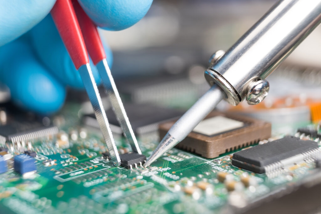
Mixed technology in PCB design refers to the integration of different component mounting methods on a single board. Typically, this involves combining SMT components, which are soldered directly onto the surface of the board, with THT components, which are inserted through holes and soldered on the opposite side. This approach allows designers to leverage the strengths of both technologies—SMT for compactness and high-speed performance, and THT for durability and high-power applications.
Industries such as telecommunications, aerospace, and medical equipment often rely on mixed technology to create complex, high-performance circuits. However, designing these boards comes with unique challenges. Let's break down the essential considerations to ensure efficiency and reliability in your mixed technology PCB designs.
Key Considerations for Efficient Mixed Technology PCB Design
1. Component Placement and Layout Optimization
One of the first steps in designing a mixed technology PCB is planning the placement of components. SMT components are smaller and ideal for high-density areas, while THT components often require more space due to their larger size and the need for drilled holes. Proper placement ensures efficient use of board space and minimizes signal interference.
Practical Tips:
- Group SMT components together on one side of the board to streamline the surface mounting process during assembly.
- Place THT components on the opposite side or in areas where mechanical strength is critical, such as connectors or power components.
- Ensure a clearance of at least 0.5 mm between SMT and THT components to avoid soldering issues during wave soldering for THT parts.
2. Signal Integrity in Mixed Technology Designs
Signal integrity is a critical factor in PCB design technology, especially for mixed technology boards where high-speed SMT components often coexist with THT parts. Poor signal integrity can lead to issues like crosstalk, noise, and data loss, particularly in high-frequency applications.
Key Strategies:
- Keep high-speed signal traces short and direct, ideally on the SMT side of the board, to reduce impedance mismatches. For example, aim for controlled impedance values of 50 ohms for single-ended signals in high-speed designs.
- Use ground planes to separate analog and digital signals, minimizing interference between SMT and THT components.
- Avoid routing high-speed traces near THT component leads, as the drilled holes can act as sources of electromagnetic interference (EMI).
By prioritizing signal integrity, you ensure that your board performs reliably, even in demanding environments like telecommunications systems operating at frequencies above 1 GHz.
3. Thermal Management for Mixed Components
Mixed technology PCBs often include components with varying power requirements. SMT components, especially in high-density areas, can generate significant heat, while THT components like power transistors may also contribute to thermal challenges. Effective thermal management is a crucial aspect of consideration technology in PCB design.
Best Practices:
- Use thermal vias under high-power SMT components to transfer heat to a ground plane or heat sink. For instance, a grid of 0.3 mm vias spaced 1.2 mm apart can improve heat dissipation.
- Position THT components with high thermal output away from heat-sensitive SMT parts to prevent overheating.
- Consider adding copper pours or heat sinks near critical areas to distribute heat evenly across the board.
4. Manufacturing and Assembly Considerations
Designing for manufacturability (DFM) is essential to ensure that your mixed technology PCB can be assembled efficiently without errors. The combination of SMT and THT components requires careful planning to accommodate different assembly processes, such as reflow soldering for SMT and wave soldering for THT.
DFM Guidelines:
- Design with standard component sizes and footprints to avoid custom soldering setups, which can increase costs and lead times.
- Ensure that THT components are placed in a way that allows wave soldering without affecting nearby SMT parts. For example, maintain a minimum distance of 2 mm between THT pins and SMT pads.
- Clearly label component orientations and polarities on the silkscreen layer to prevent assembly mistakes.
Optimizing your design for manufacturing not only reduces production errors but also lowers costs and speeds up the assembly process, making it a key focus in PCB design technology.
5. Power Distribution and Grounding
In mixed technology PCBs, power distribution and grounding are vital to prevent noise and ensure stable operation. SMT components often require low-voltage, high-current power, while THT components might handle higher voltages. A well-designed power distribution network (PDN) is critical for consideration technology in mixed designs.
Implementation Tips:
- Use dedicated power planes or wide traces (e.g., 0.5 mm or wider for high-current paths) to deliver stable power to both SMT and THT components.
- Implement a solid ground plane to provide a low-impedance return path for signals, reducing noise and EMI.
- Place decoupling capacitors (e.g., 0.1 μF ceramic capacitors) near SMT ICs to filter out high-frequency noise.
A robust PDN ensures that your mixed technology PCB operates without power-related issues, even in complex applications.
6. Material Selection for Mixed Technology Boards
The choice of PCB material impacts the performance and reliability of mixed technology designs, especially for high-frequency or high-power applications. Standard FR-4 material is often sufficient for many designs, but specific requirements may call for advanced materials.
Material Considerations:
- For high-frequency SMT components, consider low-loss materials with a dielectric constant (Dk) of around 3.0 to 3.5 to minimize signal attenuation.
- For high-power THT components, ensure the material can withstand higher temperatures, with a glass transition temperature (Tg) of at least 170°C.
- Hybrid boards combining different materials can be used to optimize performance for both SMT and THT areas, balancing cost and functionality.
7. Testing and Validation of Mixed Technology PCBs
Testing is a crucial step to ensure that your mixed technology PCB functions as intended. Due to the combination of SMT and THT components, testing must cover a range of potential issues, from soldering defects to signal integrity problems.
Testing Strategies:
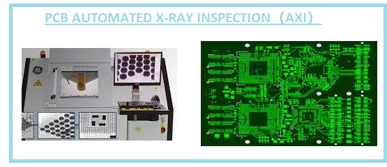
- Perform automated optical inspection (AOI) to check for soldering defects on SMT components and alignment issues with THT parts.
- Use in-circuit testing (ICT) to verify electrical connections and component functionality across the board.
- Conduct signal integrity tests with oscilloscopes to measure parameters like rise time and jitter for high-speed SMT circuits, ensuring they meet specifications (e.g., jitter below 10 ps for high-speed signals).
Thorough testing helps identify and resolve issues before the PCB moves to full-scale production, saving time and resources.
Benefits of Efficient Mixed Technology PCB Design
By addressing the considerations above, you can unlock several benefits in your mixed technology PCB projects. These include:
- Space Optimization: Combining SMT and THT allows for denser designs, ideal for compact devices.
- Cost Efficiency: Strategic component placement and DFM practices reduce manufacturing costs.
- Enhanced Performance: Proper signal integrity and thermal management ensure reliable operation in demanding applications.
- Versatility: Mixed technology supports a wide range of components, making it suitable for diverse industries.
Common Challenges and How to Overcome Them
Designing mixed technology PCBs isn't without challenges. Here are a few common issues and solutions:
- Challenge: Soldering Conflicts - Wave soldering for THT can damage SMT components. Solution: Use selective soldering techniques or assemble SMT components after THT soldering.
- Challenge: Component Interference - THT holes can disrupt SMT trace routing. Solution: Plan trace paths early and use multilayer boards if needed to avoid conflicts.
- Challenge: Design Complexity - Balancing SMT and THT requirements can be time-consuming. Solution: Use advanced design software with simulation tools to test layouts before prototyping.
Conclusion: Mastering Mixed Technology PCB Design
Designing efficient mixed technology PCBs requires careful attention to component placement, signal integrity, thermal management, and manufacturability. By focusing on these aspects of PCB design technology and consideration technology, you can create boards that are compact, reliable, and cost-effective. Whether you're working on telecommunications equipment or medical devices, the principles outlined in this guide will help you achieve high-performance results.
Start by planning your layout with both SMT and THT components in mind, and always prioritize testing to catch issues early. With the right approach, mixed technology designs can meet the demands of modern electronics while pushing the boundaries of innovation.
 ALLPCB


