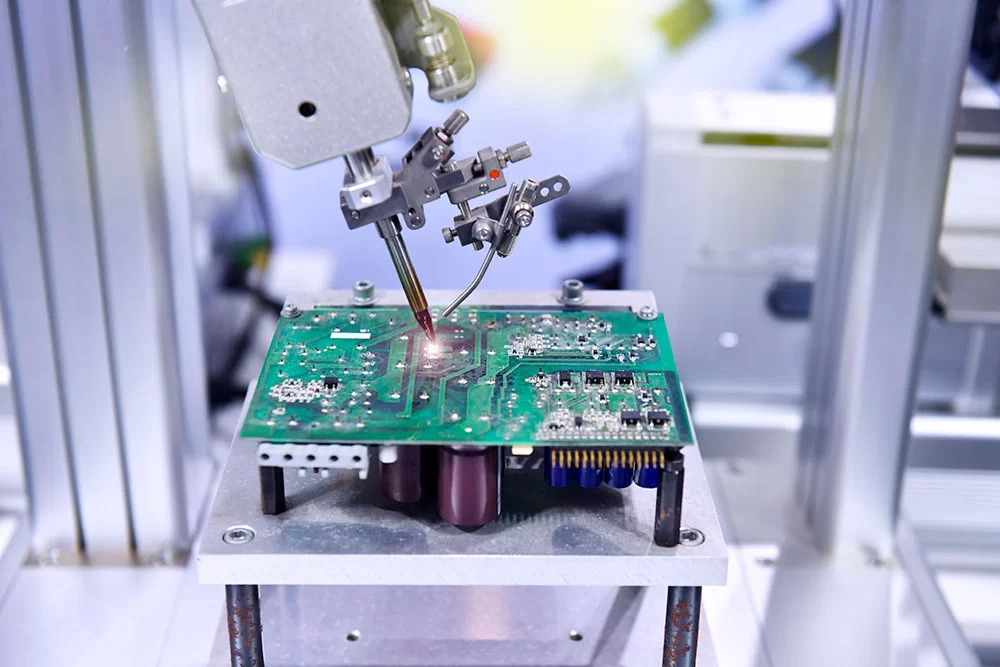
If you're an engineer looking to perfect the SMT assembly process for prototype PCB manufacturing, you're in the right place. Surface Mount Technology (SMT) assembly is a critical skill for creating compact, efficient, and high-performing electronic prototypes. In this comprehensive guide, we'll walk you through each step of SMT prototype assembly, from PCB design to reflow soldering techniques, using a pick and place machine, and ensuring precise SMT component placement. Whether you're new to this process or refining your skills, this step-by-step resource will help you achieve professional results.
What is SMT Assembly and Why Does It Matter for Prototypes?
SMT assembly is a method used to mount electronic components directly onto the surface of a printed circuit board (PCB). Unlike traditional through-hole technology, SMT allows for smaller components, higher density, and faster production, making it ideal for modern electronics and prototype PCB manufacturing. For engineers, mastering the SMT assembly process ensures that prototypes are functional, reliable, and ready for testing or small-scale production.
The benefits of SMT for prototyping include reduced board size, lower production costs for high volumes, and compatibility with automated assembly tools like pick and place machines. However, the process requires precision and attention to detail to avoid issues like component misalignment or poor soldering. Let’s dive into the detailed steps to master SMT prototype assembly.
Step 1: Designing Your PCB for SMT Assembly
Before any physical assembly begins, a well-thought-out PCB design is essential. The design phase directly impacts the success of SMT component placement and overall functionality. Start by creating a schematic that outlines the circuit's components and connections. Use design software to convert this into a PCB layout, ensuring that the pads (where components will be soldered) match the footprints of your chosen SMT components.
Key considerations during design include maintaining proper spacing between components to avoid interference during placement or soldering. For example, a minimum spacing of 0.2 mm between pads is often recommended for fine-pitch components to prevent solder bridging. Additionally, ensure that your design includes fiducial marks—small reference points on the PCB that help automated machines align components accurately during the SMT assembly process.
Step 2: Preparing the Bill of Materials (BOM) and Sourcing Components
Once your PCB design is ready, compile a Bill of Materials (BOM) that lists every component needed for the prototype. This document should include part numbers, quantities, and specifications like package size (e.g., 0402 for resistors or capacitors) to ensure compatibility with SMT assembly. Cross-check the BOM with your PCB design to avoid mismatches.
Sourcing components for prototypes can be tricky due to small order quantities. Look for suppliers that offer low minimum order quantities (MOQs) and ensure that components are available in the correct package for surface mounting. Double-check the lead time for each part to avoid delays in your prototype PCB manufacturing timeline.
Step 3: Solder Paste Application for SMT Assembly
The first physical step in the SMT assembly process is applying solder paste to the PCB. Solder paste is a mixture of tiny solder particles and flux, which helps components stick to the board and ensures a strong connection during reflow soldering. This step is critical for achieving reliable joints.
Use a stencil—a thin metal sheet with cutouts matching the PCB pads—to apply solder paste precisely. Place the stencil over the PCB and use a squeegee to spread the paste evenly across the openings. The thickness of the stencil (typically 0.1 to 0.15 mm) determines the amount of paste applied, which should be just enough to form a good solder joint without excess that could cause bridging.
After application, inspect the solder paste for consistency and alignment. Modern SMT assembly lines often use automated 3D solder paste inspection (SPI) systems to measure volume and detect defects early. For small-scale prototyping, a magnifying glass or microscope can help spot issues manually.
Step 4: SMT Component Placement with Pick and Place Machines
Once the solder paste is applied, it’s time for SMT component placement. This step involves positioning components onto the PCB pads coated with solder paste. For prototypes, this can be done manually with tweezers for very small batches, but for efficiency and precision, a pick and place machine is highly recommended.
A pick and place machine automates the process by using a robotic arm to pick components from reels or trays and place them onto the PCB with pinpoint accuracy. These machines rely on vision systems to align components with fiducial marks on the board, achieving placement accuracy within 0.01 mm for high-end models. For engineers working on prototypes, even a desktop pick and place machine can handle small runs of 50 to 100 boards efficiently, saving hours of manual labor.
Ensure that the machine is programmed with the correct component data from your BOM and PCB design files. After placement, inspect the board to confirm that components are aligned properly and seated on the solder paste.
Step 5: Reflow Soldering Techniques for Strong Connections
With components placed, the next step is reflow soldering, a process that melts the solder paste to form permanent electrical and mechanical connections between components and the PCB. Reflow soldering techniques are crucial for achieving reliable joints without damaging sensitive components.
Reflow soldering is done in a specialized oven that heats the PCB through a series of temperature zones. A typical reflow profile includes four stages:
- Preheat: Gradually raises the temperature to 150-180°C over 60-90 seconds to activate the flux and prevent thermal shock.
- Soak: Holds the temperature at 150-180°C for 60-120 seconds to ensure even heating across the board.
- Reflow: Peaks at 220-250°C (depending on solder type) for 20-40 seconds, melting the solder to form joints.
- Cooling: Lowers the temperature slowly to solidify the solder without causing stress cracks.
For prototypes, a small benchtop reflow oven can work well, but ensure it supports customizable temperature profiles to match your solder paste specifications (e.g., lead-free solder often requires higher peak temperatures around 245°C). Monitor the process closely to avoid overheating, which can damage components or cause tombstoning (when one end of a component lifts off the pad).
Step 6: Inspection and Quality Control in SMT Assembly
After reflow soldering, thorough inspection is necessary to ensure the quality of the SMT assembly process. Check for common issues like solder bridges (unintended connections between pads), cold joints (poorly formed solder connections), or misaligned components. Use a magnifying tool or microscope for manual inspection in small-scale prototyping.
For more advanced setups, Automated Optical Inspection (AOI) systems can scan the board for defects with high precision, identifying issues in seconds. X-ray inspection may also be used for hidden joints, such as under Ball Grid Array (BGA) components, to confirm solder quality. Addressing defects early prevents costly rework later in the prototype PCB manufacturing process.
Step 7: Testing and Debugging Your SMT Prototype
Once the board passes inspection, it’s time to test its functionality. Power up the prototype and use testing equipment like multimeters or oscilloscopes to measure voltages, currents, and signal integrity at key points. For digital circuits, check clock speeds (e.g., ensuring a 16 MHz oscillator operates within ±50 ppm of the target frequency) and data transmission rates.
If issues arise, debug systematically by tracing signals and checking for assembly errors like incorrect component orientation or poor solder joints. Document any problems and solutions to improve future iterations of your prototype PCB manufacturing process.
Step 8: Iterating and Refining for Production
Prototyping is an iterative process. After testing, analyze the performance of your SMT assembly and identify areas for improvement. This might involve adjusting the PCB layout for better signal routing, changing components for cost or availability, or optimizing the reflow soldering profile to reduce defects.
Keep detailed records of each prototype version, including BOM changes, assembly notes, and test results. These insights will streamline the transition from prototype to full-scale production, ensuring that your SMT assembly process is scalable and efficient.
Tips for Success in SMT Prototype Assembly
To wrap up, here are some practical tips to enhance your SMT assembly process:
- Start Small: For your first prototypes, limit the number of components to simplify assembly and debugging.
- Use Quality Materials: Invest in high-quality solder paste and components to avoid reliability issues.
- Calibrate Equipment: Regularly calibrate your pick and place machine and reflow oven to maintain accuracy.
- Practice Manual Skills: Even with automation, manual soldering or rework skills are valuable for quick fixes during prototyping.
- Stay Updated: Follow industry trends in SMT technology, such as advancements in lead-free soldering or smaller component packages like 0201.
Conclusion: Build Better Prototypes with SMT Expertise
Mastering SMT prototype assembly is a game-changer for engineers looking to create cutting-edge electronics. By following this step-by-step guide, you can navigate the complexities of the SMT assembly process, from precise SMT component placement to effective reflow soldering techniques. Whether you're using a pick and place machine or assembling by hand, attention to detail at every stage of prototype PCB manufacturing ensures a functional and reliable end product.
With practice and the right tools, you’ll gain confidence in building high-quality prototypes that pave the way for successful production runs. Start applying these steps today to elevate your engineering projects and bring innovative ideas to life.
 ALLPCB


