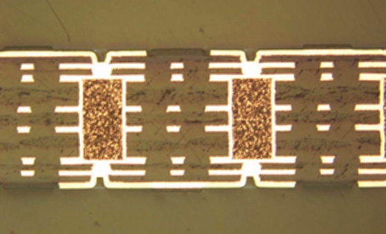
If you're looking to improve your PCB design for manufacturability (DFM), mastering copper pour techniques is essential. Copper pour, often used for ground planes, signal integrity, and thermal management, can make or break your board's performance and ease of production. In this comprehensive guide, we'll dive deep into PCB copper pour DFM, covering ground pour, signal pour, thermal relief, and copper balancing. Whether you're a beginner or a seasoned engineer, you'll find practical tips and detailed insights to optimize your designs for both functionality and manufacturing efficiency.
What Is Copper Pour in PCB Design?
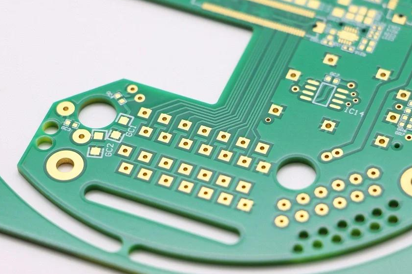
Copper pour, also known as copper fill or copper flooding, is a technique in PCB design where unused areas of a board's layer are filled with copper. This copper is typically connected to a ground or power net, serving multiple purposes like reducing noise, improving thermal dissipation, and enhancing structural integrity. For PCB copper pour DFM, proper implementation is critical to avoid manufacturing issues such as uneven etching or thermal stress during soldering.
In the following sections, we'll break down the key aspects of copper pour techniques and how to apply them effectively in your designs. Our goal is to help you create boards that are not only high-performing but also easy to manufacture.
Why Copper Pour Matters for Design for Manufacturability (DFM)
In PCB design, manufacturability is just as important as functionality. A poorly implemented copper pour can lead to issues like uneven copper distribution, which causes etching inconsistencies during fabrication. It can also result in thermal imbalances during soldering, leading to component damage or weak solder joints. By focusing on PCB copper pour DFM, you ensure that your design is optimized for both performance and production.
For example, a well-designed copper pour can reduce electromagnetic interference (EMI) by up to 20-30% in high-speed designs, according to studies on signal integrity. It can also lower thermal hotspots by distributing heat more evenly across the board, sometimes reducing peak temperatures by 10-15°C in power-intensive circuits.
Ground Pour: The Foundation of Signal Integrity
A ground pour is a type of copper pour connected to the ground net of a PCB. It acts as a reference plane for signals, reducing noise and improving signal integrity, especially in high-speed designs. Ground pour is a cornerstone of PCB copper pour DFM because it minimizes EMI and provides a low-impedance return path for currents.
To implement an effective ground pour, follow these best practices:
- Connect to Ground Net: Ensure the copper pour is tied to the ground plane with multiple vias. This reduces ground loops and maintains a consistent reference voltage.
- Avoid Isolated Islands: Remove unconnected copper areas, often called "dead copper," as they can act as antennas, picking up noise and interfering with signals.
- Clearance Rules: Maintain proper spacing (typically 8-10 mils) between the ground pour and other traces or pads to prevent shorts during manufacturing.
In high-speed designs, a solid ground pour can reduce signal crosstalk by up to 15%, based on impedance control studies. This is especially important for boards operating at frequencies above 100 MHz, where signal integrity becomes a major concern.
Signal Pour: Enhancing Performance in Specific Nets
While ground pour is the most common, signal pour refers to copper fill connected to other nets, such as power or specific signal lines. Signal pour is less common but can be useful in certain applications, like power delivery networks (PDNs) where a low-impedance path is needed for high-current signals.
For optimal signal pour in PCB copper pour DFM, consider these tips:
- Use for Power Nets: Signal pours are often applied to power planes to ensure consistent voltage delivery, especially in designs with high current draw (e.g., 5A or more).
- Minimize Loop Area: Keep the pour close to related components to reduce the loop area, which helps lower inductance and EMI.
- Balance with Ground: Always pair a signal pour with a nearby ground plane to maintain controlled impedance, ideally targeting values like 50 ohms for high-speed signals.
Signal pour can be tricky during manufacturing if not balanced properly with other layers. Uneven copper distribution can lead to warping or uneven etching, so careful planning is essential.
Thermal Relief: Balancing Heat and Connectivity
Thermal relief refers to a specific copper pour pattern around pads or vias connected to large copper areas, like ground or power planes. It’s designed to prevent heat from dissipating too quickly during soldering, which can cause poor solder joints or component damage. For PCB copper pour DFM, thermal relief is a must for manufacturability.
Here’s how to implement thermal relief effectively:
- Use Spokes: Create a pattern of thin copper traces (spokes) connecting the pad to the pour, typically 4 spokes at 90-degree angles. This limits heat flow while maintaining electrical connectivity.
- Adjust Spoke Width: For high-current applications, use wider spokes (e.g., 10-15 mils) to handle the load without overheating. For low-current pads, narrower spokes (5-8 mils) are sufficient.
- Clearance Around Pads: Ensure a clearance of at least 8 mils between the pad and the pour to avoid unintended shorts during soldering.
Without thermal relief, soldering a through-hole component to a large copper plane can require up to 50% more heat, risking damage to the component or board. Proper thermal relief ensures even heat distribution, making assembly smoother and more reliable.
Copper Balancing: Preventing Warping and Etching Issues
Copper balancing is the practice of evenly distributing copper across all layers of a PCB to prevent mechanical stress and manufacturing defects. Uneven copper distribution can cause the board to warp during fabrication or assembly due to thermal expansion differences. For PCB copper pour DFM, copper balancing is a critical step.
Follow these copper balancing methods:
- Mirror Copper on Layers: If one layer has a large copper pour, balance it with a similar pour on the opposite layer. Aim for copper coverage within 10-15% of each other across layers.
- Use Dummy Fills: In areas with little copper, add non-functional copper shapes or grids to match the density of busier areas. This helps with uniform etching during fabrication.
- Avoid Large Empty Areas: Large blank spaces can lead to over-etching in nearby copper areas. Fill these spaces with grounded copper pours if possible.
Unbalanced copper can lead to board warping of up to 0.5-1 mm across a 100 mm board, which may cause alignment issues during assembly. Balanced designs also improve thermal performance by distributing heat evenly, reducing hotspots by as much as 10°C in some cases.
Common Copper Pour Mistakes to Avoid in DFM
Even experienced designers can make mistakes with copper pour that impact manufacturability. Here are some pitfalls to watch out for:
- Dead Copper Islands: Unconnected copper areas can cause noise issues and are often flagged by manufacturers as potential defects.
- Insufficient Clearance: Tight spacing between pour and traces (less than 6 mils) risks shorts during etching or soldering.
- Overloading Thermal Relief: Too many or too wide spokes in thermal relief can negate its purpose, leading to soldering issues.
- Ignoring Layer Stackup: Failing to balance copper across layers can result in mechanical stress and board warping.
By avoiding these errors, you can save time and cost during the manufacturing process while ensuring your PCB performs as intended.
Tools and Software for Copper Pour Design
Modern PCB design software offers built-in tools to simplify copper pour and DFM optimization. Features like automatic pour generation, clearance rule checks, and copper balancing reports can streamline the process. Look for software that allows you to:
- Define custom pour shapes and net connections.
- Set thermal relief patterns with adjustable spoke width and count.
- Analyze copper density across layers for balancing.
Using these tools, you can reduce design errors and ensure your copper pour aligns with manufacturing requirements. Always generate a DRC (Design Rule Check) report to catch potential issues before sending your design for fabrication.
Conclusion: Elevate Your PCB Designs with Copper Pour Mastery
Mastering copper pour techniques is a game-changer for achieving optimal PCB DFM. By focusing on ground pour for signal integrity, signal pour for power delivery, thermal relief for soldering reliability, and copper balancing for structural stability, you can create designs that excel in both performance and manufacturability. Implementing the tips and strategies discussed—such as maintaining proper clearances, using thermal spokes, and balancing copper across layers—will help you avoid common pitfalls and ensure a smooth production process.
Whether you're working on a simple single-layer board or a complex multi-layer design, these copper pour practices will elevate your work. Start applying these techniques in your next project to see the difference in quality and efficiency. With a solid grasp of PCB copper pour DFM, you're well on your way to designing boards that meet the highest standards of functionality and ease of manufacturing.
 ALLPCB


