ALLPCB


1. Phenomenon and problem description
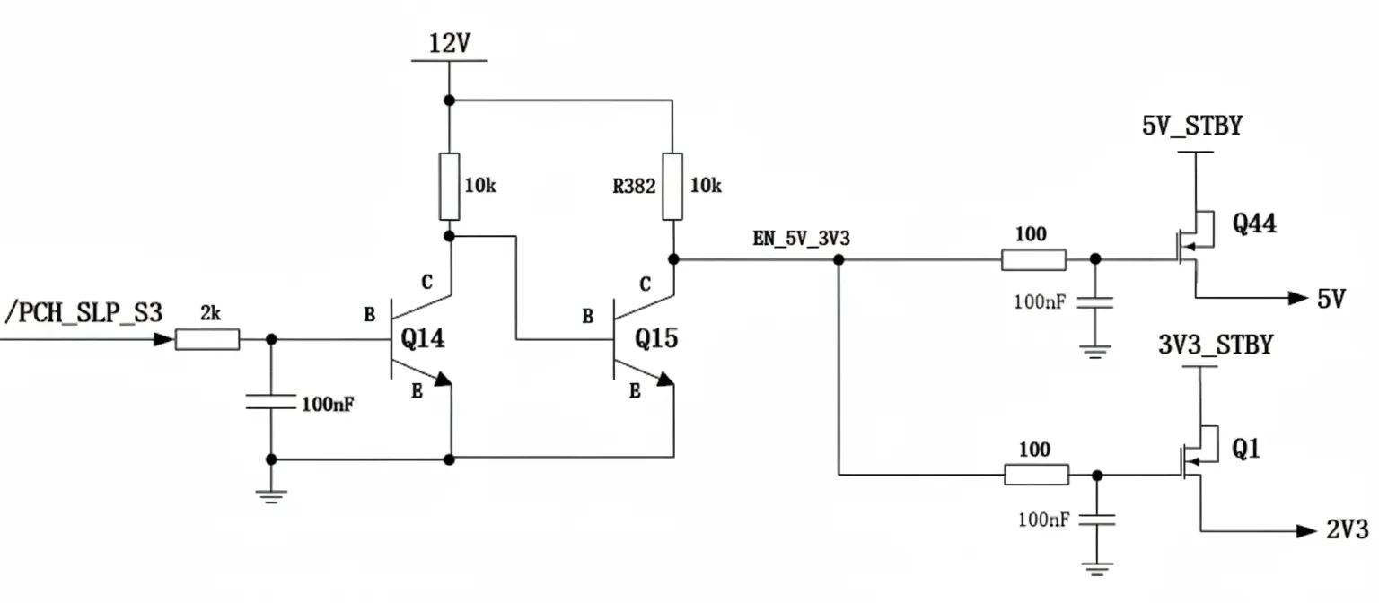
After low-temperature storage in an environmental test (chassis powered off, -40°C for 24 h), the boards were returned to room temperature (25°C) and held for 2 h before power-up. Four single-board assemblies failed to boot. Monitoring the board power rails showed the 5 V rail abnormal (measured ~2.6 V) on all faulty boards, while 3V3, 3V3_STBY, 5V_STBY and other rails were normal. After about 20 minutes (without unplugging or re-seating the faulty boards), the boards all recovered to normal operation.
In the figure below the 5 V is abnormal because Q44 is not fully conducting.

Reproducing the issue in the lab using liquid nitrogen to simulate low temperature produced intermittent results. A colleague suggested the phenomenon correlated with weather. In an ad hoc test, moisture from a fingertip was applied to the transistor package surface, then the part was cooled with liquid nitrogen; the failure consistently reproduced.
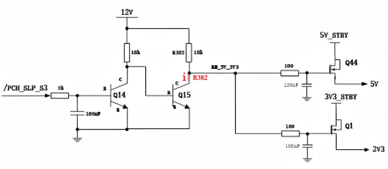
Relevant circuit:
2. Key steps and root cause analysis
Analysis:
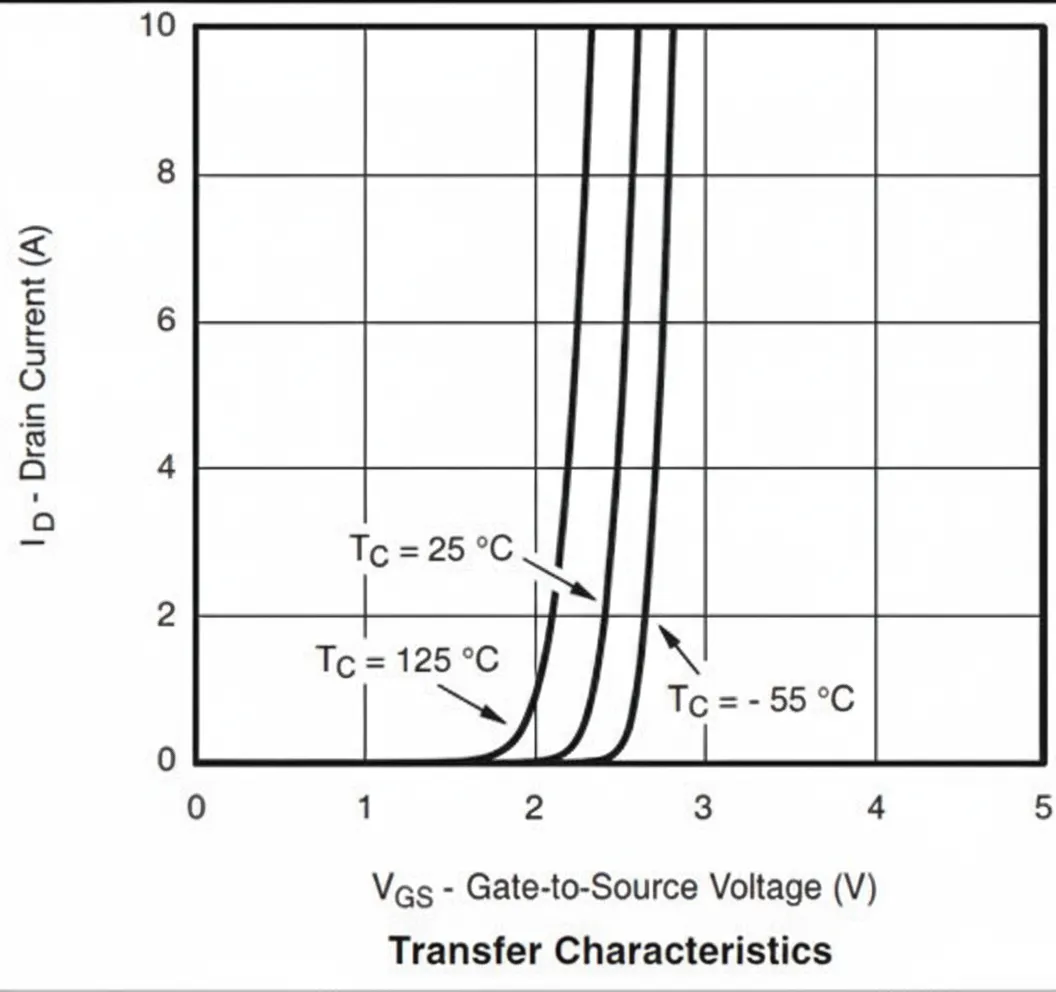
When the board fails, 5V_STBY is normal but 5V measures about 2.6 V. From the MOSFET Q44 (15060203) in the circuit, Vgs is below the threshold Vgs(th) (the device datasheet shows Vgs(th) around 2.3 V at low temperature, see Figure 2), so Q44 is not fully on. To get a normal 5 V output, the gate voltage Vg (VEN_5V_3V3) must exceed 7.3 V (5 V + 2.3 V); when the board fails, VEN_5V_3V3 < 7.3 V.
In Figure 1, the gates of the MOSFETs for 3V3 and 5V share the same enable signal EN_5V_3V3. During failure the 3V3 rail is normal, so Q1's Vgs > 2.3 V; VEN_5V_3V3 > 5.6 V (3V3 + 2.3 V).
Therefore, VEN_5V_3V3 is in the range 5.6 V to 7.3 V, which explains why 3V3 is OK while 5V is not. The following analyzes causes of the lowered VEN_5V_3V3. Figure 3 summarizes the analysis flow.
2.1 Excluding Q15 (15050026) operating in active region
Theoretical analysis:
At board startup, SLP_S3 outputs 3.3 V, so base current of Q14 is ib = (3.3 - 0.7) / 2 kΩ = 1.3 mA. If Q15 were in the active region with hFE = 100, collector current ic = 100 * 1.3 mA = 130 mA. That exceeds the saturated current limit of 1.2 mA (12 V / 10 kΩ), so the base node of Q15 should be near 0 V and Q15 should be off, not in active region. Also, transistors become harder to turn on at lower temperature, so Q15 is unlikely to be in the active region.
Measured result:
When reproducing the fault, the measured base node voltage of Q15 was only 12 mV, confirming Q15 is not in the active region.
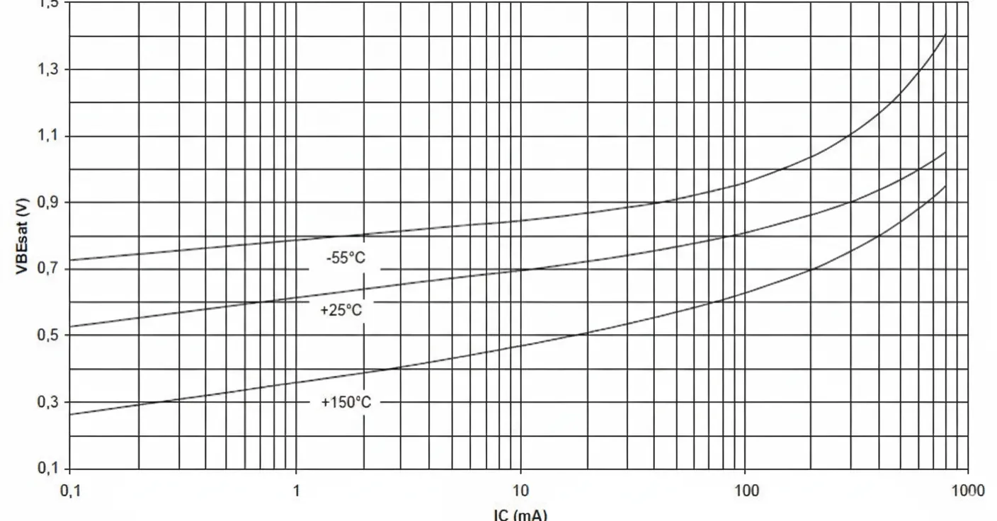
Figure 4. Ic curve for transistor Q15 (15050026)
2.2 Excluding CE or GS leakage currents as the cause
From the MOSFET datasheet (15060203), the GS leakage current is at most 100 nA (Figure 5).

Figure 5. GS leakage for MOSFET (15060203)
The CE leakage current of transistor Q15 is also at most 100 nA (Figure 6).
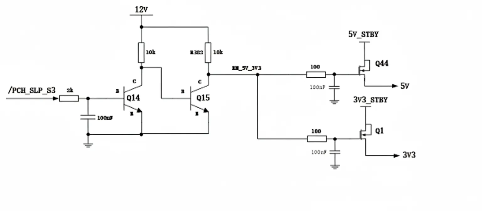
Figure 6. CE leakage for transistor Q15
Thus CE leakage of Q15 or GS leakage of Q1/Q44 would cause at most a 3 mV drop on VEN_5V_3V3 (100 nA * 3 * 10 kΩ), so leakage is not the root cause.
2.3 Confirming leakage current flows toward Q15
When the board fails, about 0.5 mA flows through R382 (5 V / 10 kΩ). The current can flow in two possible directions: I1 or I2 as shown in Figure 7. The following tests were used to determine the direction.
- Cooling Q15 with liquid nitrogen reproduces the fault. As VEN_5V_3V3 drops, measured I2 increases while I1 remains zero.
- Cooling Q1 and Q44 repeatedly did not cause VEN_5V_3V3 to drop. Both I1 and I2 remained zero during those tests.
Therefore, the transistor is sensitive to low temperature and causes the board fault. During failure, the current through R382 flows into Q15.
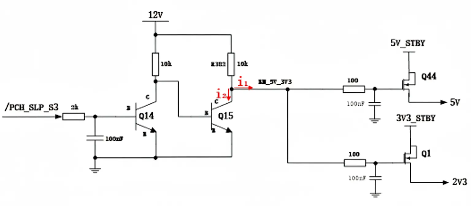
Figure 7. I1 and I2 current measurement
2.4 Analyze why Q15 produces a conductive path
- Suspect the pull-up voltage on Q15 collector (12 V) is too high;
- Possible contamination in the transistor package;
- Suspect intrinsic device behavior, test by replacing with an MOSFET in the same SOT23 package.
Because the fault is caused by Q15 at low temperature and current at R382 flows into Q15, further isolation was performed as shown in Figure 8: disconnect the downstream Q1 and Q44 (remove the 100 Ω series resistors) and tie Q15 base node directly to ground for controlled testing.
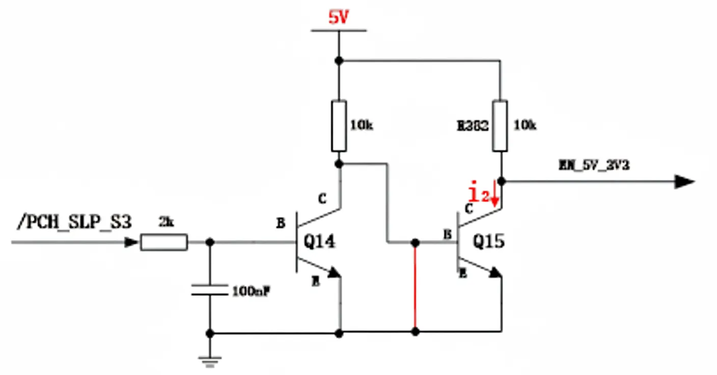
Figure 8. Pull-up voltage changed to 5 V
2.4.1 Excluding high pull-up voltage
To test whether the 12 V pull-up caused the issue, the pull-up was changed from 12 V to 5 V and Q15 was cooled with liquid nitrogen. VEN_5V_3V3 still dropped, so the pull-up voltage being too high is not the cause.
2.4.2 Excluding package contamination
Previously, some MOSFETs from certain lots showed internal contamination causing excessive leakage, but those were batch issues. Q15 was replaced with transistors from different batches and manufacturers (same type 15050026); the phenomenon persisted, so package contamination was ruled out.
2.4.3 Testing device intrinsic characteristics
Some similar circuits replace Q15 with an MOSFET in the same SOT23 package. Replacing Q15 with an MOSFET of the same package and repeating the liquid nitrogen test still reproduced the fault. VEN_5V_3V3 dropped from 5 V and sank below 2 V, remaining low for over 15 minutes. Thus the issue is not unique to the transistor type.
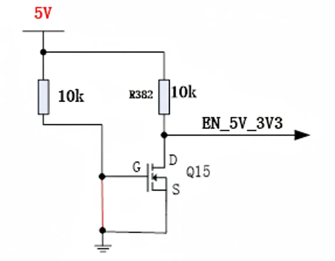
Figure 10. VEN_5V_3V3 dropped to 1.44 V under low temperature
2.4.4 Confirming SOT23 package impedance decreases at low temperature and high humidity
Measured the DS resistance of the SOT23 MOSFET on a faulty board and found about 7 kΩ; on a normal board the DS resistance measured 41 kΩ. This suggested that at low temperature the DS resistance of SOT23 MOSFETs and the CE resistance of transistors can decrease, forming a voltage divider with the 10 kΩ pull-up and lowering VEN_5V_3V3.
To verify, multiple SOT23 transistors and MOSFETs (not soldered to a PCB) were cooled with liquid nitrogen and their CE and DS resistances measured. Before cooling the measured resistance was essentially infinite (>100 MΩ). After cooling the resistances decreased, with minimum observed values around 10 kΩ.
Therefore, SOT23 transistors and MOSFETs can present reduced impedance under low temperature, leading to a voltage divider with the 10 kΩ pull-up and a drop in VEN_5V_3V3.
The manufacturer acknowledged that in low-temperature, high-humidity environments, SOT23-packaged transistors and MOSFETs can exhibit reduced impedance.
3. Conclusion, mitigation and effect
Conclusion: Under low-temperature and high-humidity conditions, small SOT23-packaged transistors or MOSFETs can exhibit low-impedance behavior. This forms a voltage divider with the 10 kΩ pull-up resistor and lowers VEN_5V_3V3. When Q15's CE impedance falls below about 14 kΩ, VEN_5V_3V3 can drop below 7 V, causing the 5 V MOSFET gate-source voltage to be insufficient for conduction and resulting in a reduced 5 V rail.
Mitigation: Reduce the pull-up resistor on Q15 collector to 1 kΩ to limit the effect of low-impedance conduction in the SOT23 device under low-temperature/high-humidity conditions.
After changing to 1 kΩ, Q15 conducts fully when on, and the pull-up is less affected. Note the resistor package and power rating should be considered because on-state current increases.
4. Lessons learned, prevention and recommendations
SOT23-packaged MOSFETs and transistors can show low RDS or RCE in low-temperature plus high-humidity conditions. When such devices are used to control switches or enable signals, avoid very large pull-up resistors. Choose lower pull-up values to ensure the output voltage meets downstream enable thresholds, and observe derating and power handling requirements for the pull-up resistor.