ALLPCB


When an IGBT operates in hard-switching mode, increasing its switching frequency causes the following problems:
- High switching losses. During turn-on the device current rises while voltage falls; during turn-off voltage rises while current falls. The overlap of voltage and current waveforms produces switching losses, which increase rapidly with switching frequency.
- Large inductive turn-off voltage spikes. When the device switches off, inductive elements in the circuit induce voltage spikes. Faster switching and higher frequency produce higher induced voltages. These voltages applied across the switch can cause IGBT module breakdown.
- Large capacitive turn-on current spikes. When the switch turns on under high voltage, the energy stored in the device's junction capacitance is discharged through the device as current. Higher frequency increases turn-on current spikes, which can overheat and damage the IGBT. In addition, a diode has a reverse-recovery interval when switching from conduction to blocking; if the switch turns on during this interval it can generate large surge currents. Higher frequency increases these surge currents and threatens device safety.
- Severe electromagnetic interference. As frequency increases, circuit di/dt and du/dt rise, increasing EMI and affecting the converter and nearby electronic equipment.
These issues limit achievable switching frequency, reduce converter efficiency, and jeopardize safe, reliable operation of switching devices. Research into soft-switching techniques provides an effective way to address these defects. Soft switching differs from hard switching. In an ideal zero-current soft turn-off, current falls to zero before voltage rises slowly to the off-state value, so turn-off loss is approximately zero. Because current is already zero before turn-off, inductive turn-off problems are eliminated. In an ideal zero-voltage soft turn-on, voltage falls to zero before current rises slowly to the on-state value, so turn-on loss is approximately zero; the device junction capacitance voltage is also zero, solving capacitive turn-on problems. Also, diode reverse-recovery has completed before turn-on, so reverse-recovery issues no longer occur. Reduced di/dt and du/dt mitigate EMI.
Soft switching uses LC buffering and absorption so that device current (or voltage) varies in a sinusoidal or quasi-sinusoidal manner. When current crosses zero the device is turned off; when voltage crosses zero the device is turned on, achieving near-zero switching loss.
Soft-switching significantly improves the operating conditions of power switches, enabling higher-frequency converters, improving device reliability and safety, and reducing voltage and current stress on switches. It also helps reduce converter size and weight and lowers EMI.
1. Snubber Absorption Principle
Snubber circuits (RC absorption networks) are mainly used to suppress overvoltage and du/dt or overcurrent and di/dt of IGBT cells inside a module, while reducing IGBT switching losses. Because the required resistor and capacitor power ratings and sizes are large, these circuits are not typically integrated inside IGBT modules. Therefore, snubber circuits are implemented at system level. Capacitors store the electromagnetic energy of an overvoltage as electrostatic energy, and resistors prevent resonance between capacitance and inductance. Without a snubber, turn-on current will rise rapidly with large di/dt, turn-off exhibits large du/dt and high overvoltage, which can damage the IGBT.
Active snubber circuits add auxiliary switches to reduce switching losses, but this increases the complexity of the main circuit and the control circuit, reducing cost-effectiveness and reliability. The RCVD snubber is structurally simplest and cheapest, but resistors dissipate energy so efficiency is low and overall performance among soft-switch techniques is poorest. Resonant converters can achieve ZVS or ZCS and reduce switching loss, but require sufficiently large resonant energy to create ZVS/ZCS conditions; resonant circuits have large circulating currents and must operate under specific soft-switch controller signals, which increases conduction loss and cost and reduces reliability. Unlike these methods, passive lossless snubber circuits do not use active devices; their efficiency is comparable to active snubbers and resonant converters, they have low EMI, low cost, good performance, and high reliability, and therefore they are widely used.
Although passive lossless snubbers cannot, by advancing or delaying main-switch timing as active soft-switch schemes do, actively absorb or supply energy to create true ZVS or ZCS conditions, they shift the voltage and current waveforms during switching to minimize their overlap area and thus significantly reduce switching loss. While discharge loss of device parasitic junction capacitance cannot be eliminated by passive lossless snubbers, that loss is much smaller than other switching losses and has limited impact on overall efficiency. Compared with other soft-switch schemes, passive lossless snubbers do not add auxiliary active-device losses; therefore, for the same reduction in switching-loss power, passive lossless snubbers achieve greater overall efficiency improvement. For this reason, passive lossless snubbers are widely applied in PWM converters.
Lossless absorption networks can reuse energy absorbed from input or output circuits, typically by feeding it back to the power supply or load, or by circulating it internally within the absorption network.
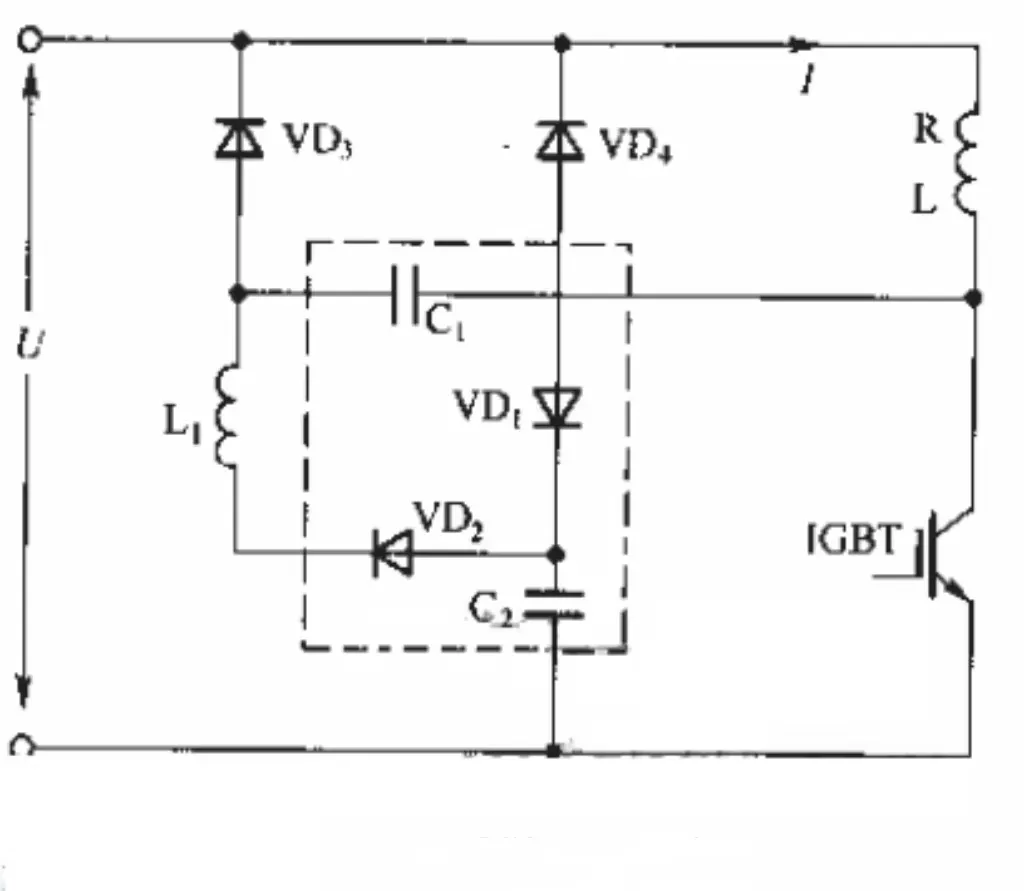
When the IGBT turns off the circuit begins to operate: load current charges snubber capacitor C2 through diode VD1, while capacitor C1 (charged to U during conduction) discharges through VD3, returning energy to the load and providing a freewheeling path for load current. The IGBT collector current gradually decreases. When C2 charges to U and C1 discharges to zero, VD3 blocks and the inductive load current flows through the main freewheeling diode VD4. Because the voltage across C2 cannot change instantaneously, it effectively limits the IGBT collector voltage rise rate du/dt, reducing voltage stress on the IGBT while transferring collector current into the snubber circuit, thereby reducing turn-off loss.
During IGBT turn-on, diodes VD1 and VD3 are reverse-biased, and C2, L1 and C1 form a resonant circuit. Voltage U is applied across L1 in the absorption network; current flows from C2 through L1 and VD2 to charge C1. When C2 discharges to zero and C1 charges to U, the current in L1 reaches zero, series diode VD2 blocks, resonance ends, and C1 stores energy in preparation for the next IGBT turn-off.
During this turn-on interval, the load inductance L, collector bus inductance, various stray inductances and L1 limit the collector current, effectively reducing the IGBT collector current rise rate di/dt, lowering current stress and turn-on loss. Thus, the snubber reduces switching losses and the voltage and current stress on devices.
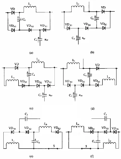
2. Topology Classification
Over the past decades many passive lossless snubber topologies have been developed and can be described by a set of attributes. They can be classified into two groups: minimum voltage stress (MVS) units, as in figures (a) and (b); and non-minimum voltage stress (Non-MVS) units, as in figures (c), (d), (e) and (f). MVS units use only a single inductor and a relatively small capacitor to minimize voltage stress on the main switch, but their soft-switching range is limited. Non-MVS units add an extra inductor, which increases voltage stress on the main switch but, for the same inductance and capacitance, provides a larger soft-switching range and higher efficiency at low power.