 ALLPCB


Gold plating is a critical process in PCB manufacturing, ensuring durability, conductivity, and corrosion resistance for electronic components. Whether you're troubleshooting soft gold plating issues, aiming to avoid plating defects, or seeking tips to improve gold plating quality, following best practices is essential. In this comprehensive guide, we’ll dive into the key strategies for achieving flawless gold plating results, addressing common gold plating issues, and sharing actionable gold plating tips and tricks to elevate your manufacturing process.
Why Gold Plating Matters in PCB Manufacturing
Gold plating plays a vital role in enhancing the performance and longevity of printed circuit boards (PCBs). It provides a thin, protective layer that prevents oxidation, ensures excellent electrical conductivity, and withstands harsh environmental conditions. This makes it ideal for high-reliability applications like aerospace, medical devices, and telecommunications. However, achieving consistent quality requires attention to detail and adherence to best practices, especially when dealing with soft gold plating or troubleshooting defects.
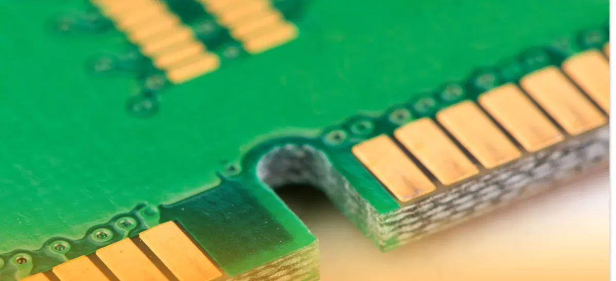
Types of Gold Plating: Soft Gold vs. Hard Gold
Before diving into best practices, it’s important to understand the two primary types of gold plating used in PCB manufacturing:
- Soft Gold Plating: Known for its purity and flexibility, soft gold is ideal for wire bonding applications. It typically has a purity of 99.9% and is less durable than hard gold, making it prone to wear if not handled properly. Soft gold plating troubleshooting often focuses on adhesion and surface contamination issues.
- Hard Gold Plating: This type includes alloying elements like cobalt or nickel, making it more durable and suitable for high-wear areas like edge connectors. It’s less pure (around 99.7%) but offers better resistance to abrasion.
Choosing the right type depends on your application. For instance, soft gold is preferred for delicate bonding processes, while hard gold excels in areas requiring frequent contact.
Best Practices for Gold Plating in PCB Manufacturing
To achieve optimal results and avoid common gold plating issues, follow these proven best practices during the plating process. These steps will help in avoiding plating defects and improving gold plating quality across your projects.
1. Thorough Surface Preparation
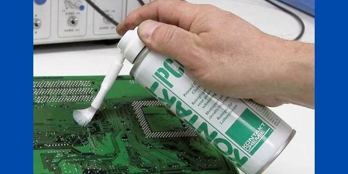
The foundation of high-quality gold plating lies in proper surface preparation. Any contamination, such as oils, dust, or oxides, can lead to poor adhesion and defects like peeling or uneven coating. Here’s how to prepare the surface:
- Clean the PCB thoroughly using a combination of alkaline cleaners and micro-etching solutions to remove organic and inorganic residues.
- Ensure the copper layer beneath is free of oxidation, as this can interfere with the nickel underlayer (if used) and gold adhesion.
- Rinse with deionized water to prevent ionic contamination that could cause defects.
Proper preparation reduces the risk of gold plating issues by up to 30%, based on industry observations, ensuring a smooth and uniform coating.
2. Optimize Plating Thickness for Your Application
Gold plating thickness directly impacts performance and cost. Too thin a layer may not provide adequate protection, while excessive thickness increases material costs without added benefits. Recommended thicknesses vary by application:
- For soft gold used in wire bonding, a thickness of 0.25 to 0.5 microns is often sufficient.
- For hard gold on edge connectors, aim for 0.75 to 1.25 microns to withstand repeated insertions (up to 200 cycles or more, depending on the design).
Monitor thickness using X-ray fluorescence (XRF) testing to ensure consistency. Over-plating can also lead to stress in the layer, causing cracks or peeling—common gold plating issues that require troubleshooting.
3. Use High-Quality Plating Solutions and Equipment
The quality of the plating bath and equipment significantly affects the outcome. For soft gold plating, ensure the electrolyte solution is free of impurities and maintained at the correct temperature (typically 50-60°C). Hard gold plating may require specific additives to achieve the desired durability.
- Regularly filter the plating solution to remove contaminants that could cause pitting or uneven deposition.
- Maintain consistent current density (around 1-5 A/dm2 for soft gold) to avoid burning or over-deposition.
- Calibrate equipment frequently to ensure uniform application across the board.
Investing in quality materials and maintenance can reduce plating defects by ensuring a stable and controlled process.
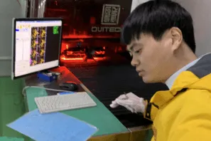
4. Implement Strict Quality Control Measures
Quality control is non-negotiable for avoiding plating defects and improving gold plating quality. After plating, conduct the following checks:
- Visual Inspection: Look for discoloration, unevenness, or pinholes in the gold layer.
- Adhesion Testing: Use tape tests or thermal shock tests to confirm the gold adheres well to the substrate.
- Thickness Measurement: Use non-destructive testing methods like XRF to verify the gold layer meets specifications.
Implementing these checks can catch up to 90% of potential defects before the PCBs move to assembly, saving time and resources.
Soft Gold Plating Troubleshooting: Common Issues and Fixes
Soft gold plating, while excellent for specific applications, can present unique challenges. Below, we address common gold plating issues and provide actionable solutions to improve outcomes.
Issue 1: Poor Adhesion
Poor adhesion often results from inadequate surface preparation or contamination. If the gold layer peels or flakes, consider these fixes:
- Revisit the cleaning process to ensure no residues remain on the surface.
- Check for oxidation on the nickel underlayer (if applicable) and address it with a light etch.
- Verify the plating bath chemistry, as imbalances can weaken bonding.
Issue 2: Uneven Deposition
Uneven gold distribution can lead to inconsistent performance. This issue often stems from improper current distribution or bath agitation.
- Adjust the anode-to-cathode spacing to ensure uniform current flow.
- Increase bath agitation to prevent localized depletion of gold ions.
- Monitor current density to avoid high spots that cause over-plating in certain areas.
Issue 3: Pitting or Porosity
Pitting appears as small holes or voids in the gold layer, compromising corrosion resistance. This defect is often linked to contamination or gas entrapment.
- Filter the plating solution regularly to remove particles.
- Reduce hydrogen gas formation by optimizing current density and bath temperature.
- Ensure proper rinsing between process steps to avoid trapped residues.
Avoiding Plating Defects: Proactive Tips and Tricks
Prevention is always better than correction. Here are some gold plating tips and tricks to help you avoid plating defects from the start:
- Control Environmental Factors: Maintain a cleanroom environment to minimize dust and airborne contaminants during plating. Humidity levels should be kept between 40-60% to prevent moisture-related issues.
- Use a Nickel Barrier Layer: For most gold plating applications, a nickel underlayer (2-5 microns thick) prevents copper diffusion and enhances adhesion.
- Handle with Care: After plating, use gloves to avoid fingerprint oils or scratches on the gold surface, which can lead to corrosion over time.
- Store Properly: Store gold-plated PCBs in a dry, temperature-controlled environment to maintain integrity before assembly.
Improving Gold Plating Quality: Advanced Strategies
Beyond the basics, there are advanced techniques to further elevate your gold plating results. These strategies focus on precision and long-term reliability.
1. Adopt Electroless Nickel Immersion Gold (ENIG)
ENIG is a popular process that combines a nickel barrier with an immersion gold layer. It offers excellent solderability and flatness, making it ideal for fine-pitch components. Ensure the immersion gold layer is kept thin (0.05-0.1 microns) to avoid issues like black pad syndrome, where nickel corrosion affects solder joints.
2. Monitor Bath Life and Composition
Over time, plating baths degrade due to metal depletion or contaminant buildup. Replace or refresh the solution based on usage (typically after 5-10 metal turnovers, depending on the bath type). Regular testing with atomic absorption spectroscopy can help maintain optimal chemistry.
3. Train Your Team
Human error is a significant factor in gold plating defects. Provide ongoing training for staff on proper handling, equipment operation, and quality control procedures to minimize mistakes and ensure consistent results.
Conclusion: Mastering Gold Plating for Superior PCBs
Gold plating is a cornerstone of high-performance PCB manufacturing, but achieving flawless results requires meticulous attention to detail. By following the best practices outlined in this guide—such as thorough surface preparation, precise thickness control, and proactive troubleshooting—you can avoid common gold plating issues and ensure top-tier quality. Whether you’re focusing on soft gold plating troubleshooting, avoiding plating defects, or seeking gold plating tips and tricks, these strategies will help you improve gold plating quality and deliver reliable, long-lasting products.
Implementing these practices not only enhances the durability and conductivity of your PCBs but also builds trust with clients who rely on your components for critical applications. Start applying these techniques today to see a marked improvement in your gold plating process.


