 ALLPCB


Designing flexible printed circuit boards (flex PCBs) for manufacturability is crucial to ensure a smooth assembly process, reduce costs, and improve reliability. By following DFM guidelines for flex PCBs, optimizing flex PCB layout for assembly, and focusing on minimizing assembly steps in flex design, you can create efficient and high-quality products. Additionally, understanding tooling considerations for flex PCB assembly and implementing effective fiducial placement strategies for flex PCBs can streamline production and enhance accuracy. In this comprehensive guide, we’ll dive deep into these topics to help engineers and designers achieve success in flex PCB projects.
What is Designing for Manufacturability (DFM) in Flex PCBs?
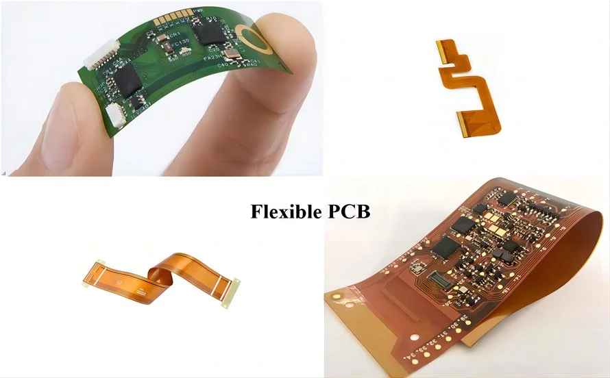
Designing for Manufacturability (DFM) refers to the practice of creating PCB designs that are easy and cost-effective to produce. For flex PCBs, which are used in applications requiring bending and dynamic movement, DFM becomes even more critical. These boards are often found in wearable devices, medical equipment, and compact electronics where space and flexibility are key. Poor DFM practices can lead to manufacturing defects, increased costs, and delays in production.
In this blog, we’ll explore actionable DFM guidelines for flex PCBs, tips for optimizing layouts, and strategies to simplify assembly. Whether you’re a seasoned engineer or new to flex PCB design, this guide offers practical insights to improve your workflow and ensure high-quality results.
Why DFM Matters for Flex PCB Assembly
Flex PCBs differ from rigid boards due to their ability to bend and conform to unique shapes. However, this flexibility introduces unique challenges during manufacturing and assembly. Without proper DFM guidelines for flex PCBs, issues like material stress, improper bending, or component misalignment can arise. DFM helps address these challenges by ensuring the design aligns with manufacturing capabilities, reducing errors and scrap rates.
For instance, a poorly designed flex PCB might have traces that crack under repeated bending, or components placed in areas prone to stress, leading to failure rates as high as 20-30% in some cases. By prioritizing DFM, you can minimize such risks and create reliable designs that perform well in real-world applications.
Key DFM Guidelines for Flex PCBs
Following DFM guidelines for flex PCBs is essential to ensure your design can be manufactured efficiently. Below are some critical principles to keep in mind during the design phase.
1. Material Selection for Flexibility and Durability
Choosing the right materials is the foundation of a successful flex PCB design. Polyimide is a common substrate material for flex PCBs due to its high thermal stability and flexibility. Ensure that the material thickness (often between 1 mil to 5 mil) matches the bending requirements of your application. Thinner materials offer greater flexibility but may compromise durability, while thicker materials provide strength at the cost of reduced bendability.
Additionally, consider adhesive-less copper laminates to reduce stress during bending. Adhesives can delaminate under repeated flexing, leading to failures. By selecting appropriate materials, you set the stage for a manufacturable and reliable design.
2. Bend Radius and Stress Management
One of the most critical DFM guidelines for flex PCBs is adhering to proper bend radius limits. A general rule of thumb is to maintain a bend radius of at least 10 times the thickness of the flex PCB. For a 2 mil thick board, this means a minimum bend radius of 20 mil. Tighter bends can cause trace cracking or material fatigue over time.
Avoid placing vias or components in high-stress bend areas, as they are prone to damage. Instead, use curved traces rather than sharp angles to distribute stress evenly. These practices help extend the lifespan of the board, especially in dynamic applications.
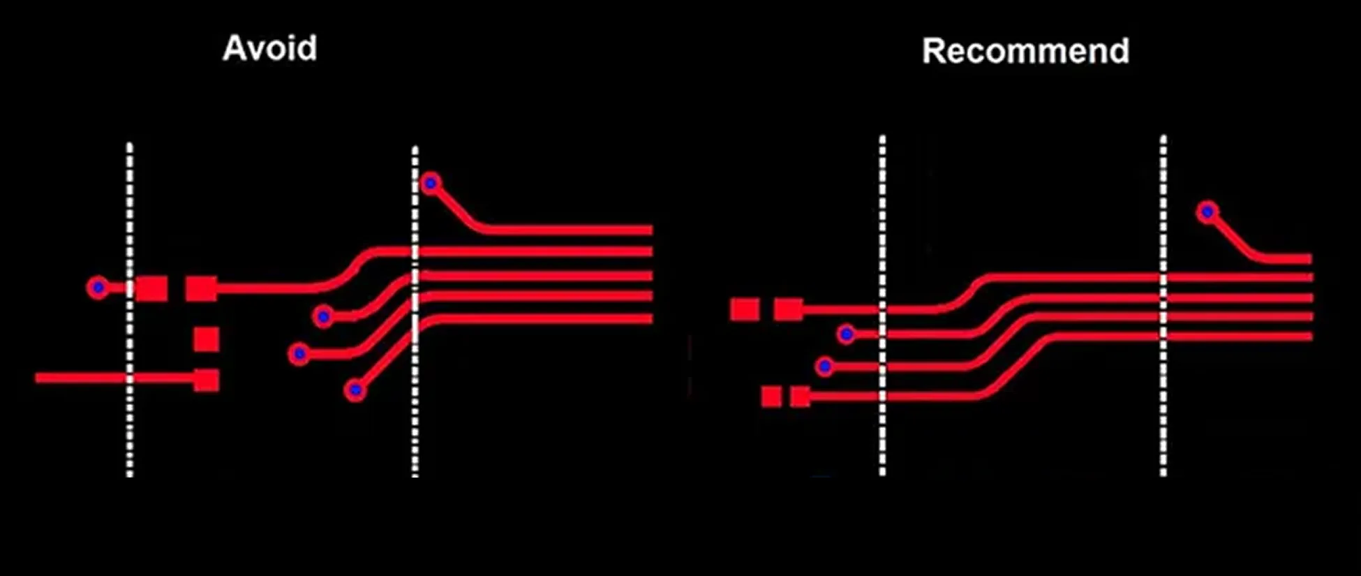
3. Trace Width and Spacing for Reliability
Trace width and spacing are crucial for both electrical performance and manufacturability. For flex PCBs, wider traces (e.g., 6-8 mil) are preferred in bend areas to reduce the risk of cracking. Maintain adequate spacing (at least 6 mil) between traces to prevent short circuits during bending or manufacturing variations.
Additionally, consider staggering traces on multilayer flex PCBs to avoid overlapping stress points. These small adjustments can significantly improve the board’s reliability and ease of production.
Optimizing Flex PCB Layout for Assembly
Optimizing flex PCB layout for assembly is a key step in reducing production time and costs. A well-thought-out layout ensures that components are placed efficiently, soldering is straightforward, and the board can be handled easily during assembly. Let’s explore some strategies to achieve this.
1. Component Placement for Accessibility
Place components in areas that are easy to access during assembly. Avoid positioning parts in tight bend zones, as this can complicate soldering and increase the risk of damage. For surface-mount components, ensure pads are large enough (e.g., at least 10 mil annular ring) to accommodate manufacturing tolerances and provide a strong connection.
Group similar components together to streamline the pick-and-place process during assembly. This reduces machine setup time and minimizes errors, making the assembly process more efficient.
2. Use of Stiffeners for Support
Stiffeners are rigid materials added to specific areas of a flex PCB to provide mechanical support during assembly and operation. They are especially useful in areas with heavy components or connectors. For example, a stiffener made of FR4 material (0.010” to 0.020” thick) can be added under a connector to prevent bending and ensure proper alignment during soldering.
Integrating stiffeners into your layout not only aids assembly but also enhances the durability of the final product. Be sure to specify stiffener locations clearly in your design files to avoid miscommunication with manufacturers.
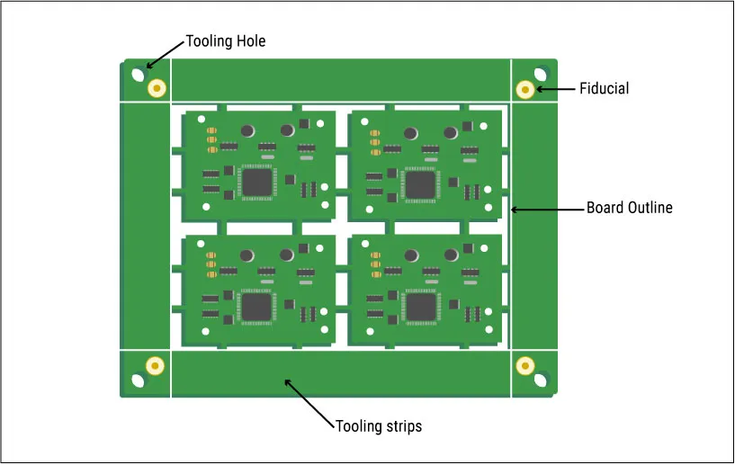
3. Panelization for Efficient Production
Panelization involves arranging multiple flex PCBs on a single panel for manufacturing. This reduces material waste and speeds up assembly. When designing for panelization, leave sufficient spacing (at least 0.1 inch) between boards to allow for clean separation after assembly. Also, include tooling holes or slots in the panel to aid in alignment during production.
Minimizing Assembly Steps in Flex Design
Minimizing assembly steps in flex design is a powerful way to save time and reduce costs. The fewer steps required to assemble a board, the lower the chances of errors and defects. Here are some tips to simplify the process.
1. Reduce Component Count
Where possible, use multifunctional components to reduce the total number of parts on the board. For example, instead of using separate resistors and capacitors, consider integrated solutions that combine multiple functions into a single package. Fewer components mean fewer placement and soldering steps, streamlining the assembly process.
2. Design for Automated Assembly
Automated assembly machines, such as pick-and-place systems, are faster and more precise than manual assembly. Design your flex PCB with automation in mind by using standard component sizes and ensuring clear markings for polarity and orientation. Avoid odd-shaped or oversized components that may require manual handling, as this can slow down production.
3. Simplify Soldering Requirements
Opt for surface-mount technology (SMT) over through-hole components whenever possible, as SMT is more compatible with automated assembly. Additionally, use larger pad sizes and avoid fine-pitch components (below 0.4 mm) unless absolutely necessary, as they can complicate soldering and increase defect rates.
Tooling Considerations for Flex PCB Assembly
Tooling considerations for flex PCB assembly play a significant role in ensuring accurate and efficient production. Proper tooling helps align the board during manufacturing and assembly, reducing errors and improving yield. Here are some key factors to consider.
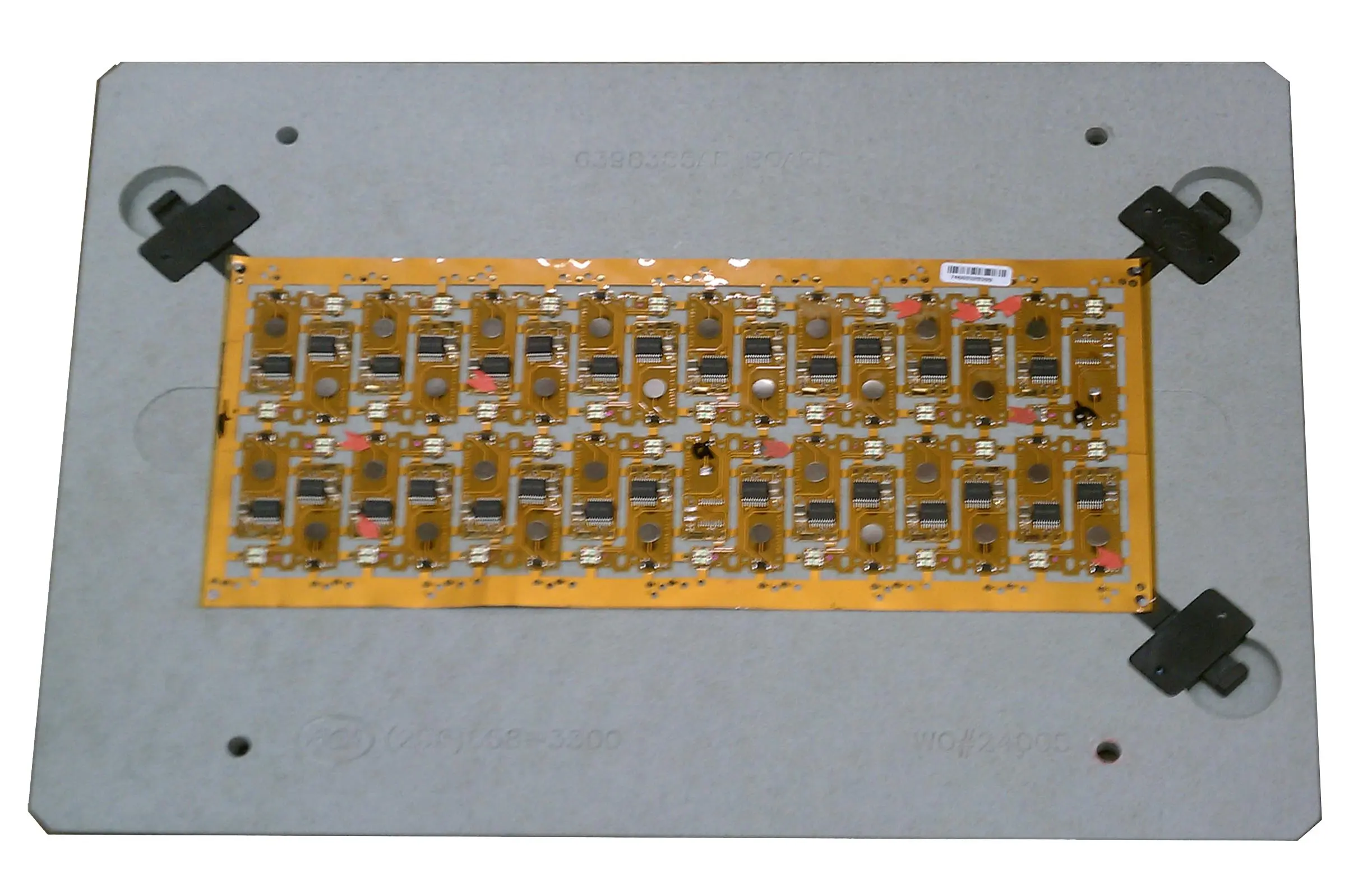
1. Custom Fixtures for Flex PCBs
Unlike rigid PCBs, flex PCBs can deform easily, making alignment challenging during assembly. Custom fixtures or carriers can hold the board in place, ensuring precise component placement and soldering. These fixtures are often made from materials like aluminum or high-temperature plastics to withstand the assembly process.
Work with your manufacturing partner to design fixtures that match the specific shape and size of your flex PCB. This upfront investment can save significant time and reduce errors during production.
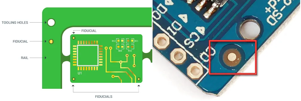
2. Tooling Holes for Alignment
Include tooling holes in your flex PCB design to aid in alignment during assembly. These holes (typically 0.125” in diameter) should be placed in non-critical areas of the board and spaced evenly to ensure stability. Tooling holes are especially important for multilayer flex PCBs, where precise layer alignment is critical.
3. Edge Clearance for Handling
Leave sufficient edge clearance (at least 0.2 inches) around the board to allow for safe handling and fixture attachment. This prevents damage to critical areas during assembly and ensures the board can be processed without issues.
Fiducial Placement Strategies for Flex PCBs
Fiducial placement strategies for flex PCBs are essential for achieving accurate component placement during automated assembly. Fiducials are reference marks on the board that machines use to orient themselves. Proper placement ensures precision, especially for flex PCBs, which can shift or deform during handling.
1. Strategic Fiducial Locations
Place at least three fiducial marks on the board in a triangular pattern to provide accurate reference points for the assembly machine. Position them near the corners of the board or panel, away from bend areas, to avoid distortion. For larger panels, include additional fiducials near high-density component areas to improve local accuracy.
2. Fiducial Size and Shape
Fiducials should be circular with a diameter of 0.040” to 0.060” and surrounded by a clear zone (at least 0.080” diameter) free of other markings or traces. This ensures the machine vision system can detect them easily. Use a solid copper dot with a solder mask opening for best visibility.
3. Consistency Across Panels
For panelized designs, ensure fiducials are placed consistently across all boards in the panel. This allows the assembly machine to use the same reference points for every board, reducing setup time and improving accuracy.
Best Practices for Successful Flex PCB Assembly
To wrap up, let’s summarize some overarching best practices for designing flex PCBs with manufacturability in mind. These tips combine the concepts discussed above into a cohesive approach.
- Collaborate early with your manufacturing partner to align on design rules and capabilities.
- Perform thorough simulations and testing to validate bend radius, stress points, and electrical performance before production.
- Use design software with built-in DFM checks to catch potential issues like improper trace spacing or component placement.
- Document all design specifications clearly, including material choices, stiffener locations, and fiducial placements, to avoid miscommunication.
Conclusion
Designing flex PCBs for manufacturability is a critical step in creating reliable, cost-effective, and high-performing electronics. By adhering to DFM guidelines for flex PCBs, optimizing flex PCB layout for assembly, and minimizing assembly steps in flex design, you can streamline production and reduce errors. Additionally, paying attention to tooling considerations for flex PCB assembly and implementing effective fiducial placement strategies for flex PCBs ensures precision and efficiency throughout the process.
At ALLPCB, we’re committed to supporting engineers and designers in achieving success with their flex PCB projects. By applying the strategies and best practices outlined in this guide, you’ll be well-equipped to tackle the unique challenges of flexible board assembly and deliver outstanding results in your applications.


