ALLPCB


Overview of the chip design process
The chip design process typically includes the following main stages:
- Requirement analysis: Define the design goals and constraints, including performance, power, and functional requirements. This stage involves aligning requirements with stakeholders and specifying interfaces and constraints.
- Architectural design: Define the overall system architecture, identify functional blocks, interfaces, interconnects, and data flows. System-level tradeoffs are made to optimize performance, area, and power.
- Logic design: Describe the circuit behavior using hardware description languages such as Verilog or VHDL, then perform logic synthesis, timing optimization, and RTL-to-gates implementation.
- Physical design: Transform the synthesized netlist into a physical layout. Tasks include floorplanning, placement, routing, clock-tree synthesis, and application of design rules to meet timing, signal integrity, and power goals.
- Verification and simulation: Verify functional correctness and performance through functional verification, timing analysis, power analysis, and electromagnetic compatibility checks. This stage includes extensive simulation and formal checks.
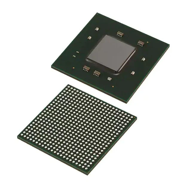
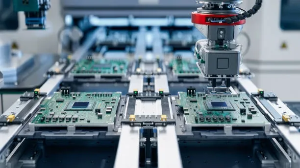
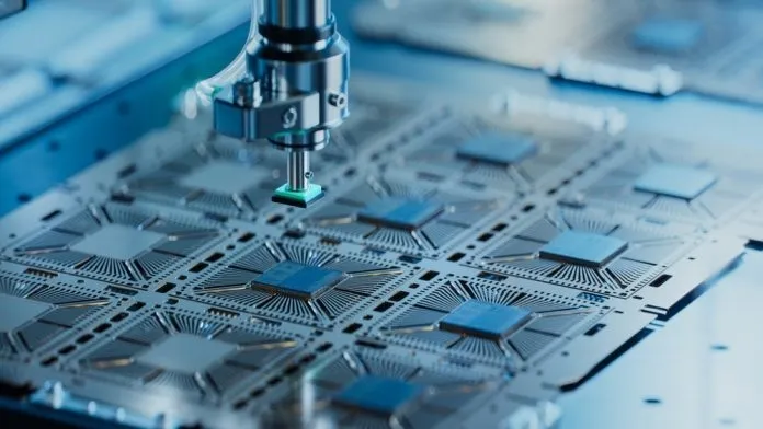
- Manufacturing and packaging: Prepare masks, wafer fabrication, probe testing, and packaging. The objective is to produce silicon that meets specified electrical and mechanical requirements.
- Testing and debug: Test fabricated devices for functionality, performance, and reliability. Debug failures, iterate on design or process fixes, and qualify the product.
- Volume production and product launch: Ramp manufacturing to volume, stabilize yields, and support product introduction and lifecycle activities.
Each stage typically requires multiple iterations and close coordination among design, verification, physical implementation, and test teams to ensure manufacturability and meet target specifications.
Key challenges in 5G chip design
Designing chips for 5G applications presents several major challenges:
- System complexity: 5G requires support for wider bandwidths, multiple frequency bands, and advanced modulation schemes, which increases system complexity and the required signal processing and computation.
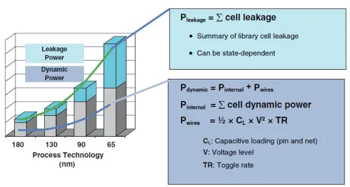
- Low power operation: High data rates and intensive signal processing increase power consumption and thermal load, especially for mobile and edge devices. Power management and energy-efficient architectures are critical to meet battery life and thermal constraints.
- RF design: Support for higher frequency bands and beamforming increases RF frontend complexity. Antenna integration, analogue/digital coexistence, linearity, and RF calibration are major challenges that affect performance and reliability.
- Packaging and interconnect: Higher integration density and fast signaling require advanced packaging, high-density interconnects, and careful signal-routing strategies to preserve signal integrity and minimize latency and power loss.
- Security: 5G systems handle sensitive data and require robust security features. Chip-level security considerations include secure boot, cryptographic acceleration, key management, and protections against side-channel and physical attacks.
Addressing these challenges requires cross-disciplinary solutions spanning architecture, RF, analogue/mixed-signal design, physical implementation, and system-level power and security engineering.