ALLPCB


This article reviews chip design, tapeout, verification, fabrication, and cost. Tapeout is like a major exam for a chip design: it validates whether the design can be manufactured as intended.
Tapeout is the key stage in semiconductor manufacturing where the finalized design is handed over to a foundry to produce wafers. It verifies whether the manufactured chips meet design requirements or need further optimization. If samples meet specifications, the design can move to volume production.
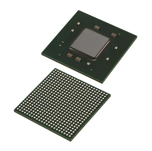
1. Wafer terminology
- chip, die, device, circuit, microchip, or bar: these terms refer to the microchip patterns that occupy most of the wafer surface.
- scribe line or street: the separation areas on the wafer that divide individual chips. Scribe lines are usually blank, but some companies place alignment marks or test structures there.
- engineering die and test die: these differ from regular production dies. They include special devices and circuit blocks used for electrical testing of wafer process steps.
- edge die: dies at the wafer edge that suffer partial masking, resulting in area loss. Moving to larger wafer diameters reduces fractional edge-die waste, which is one factor driving the industry toward larger wafers.
- wafer crystal plane: a wafer cross section shows the lattice structure beneath devices. Device edges are aligned relative to the crystal orientation.
- wafer flats and notch: some wafers have major and minor flats indicating a P-type <100> crystal orientation, while 300 mm and 450 mm wafers typically use a notch for crystal-orientation identification. These features also assist in wafer orientation and alignment during some process steps.
Related Reading: Metastability and Synchronizers in Chip Design
2. Tapeout modes: Full Mask and MPW
Full Mask and MPW (Multi Project Wafer) are two tapeout approaches. Full Mask uses a full set of masks dedicated to a single design. MPW places multiple projects sharing the same process on one wafer so several designs can be manufactured in a single run.
- Full Mask: all masks in the manufacturing flow serve a single design. One wafer can yield thousands of dice that, after packaging, support large-volume demand.
- MPW: similar to PCB panelization for prototypes, MPW combines multiple designs that use the same process on a single wafer. Each design typically receives several dozen sample dies, sufficient for prototype testing. MPW can reduce tapeout cost by 90%–95%, significantly lowering R&D expense.
- Foundries usually schedule several MPW runs per year, often called shuttles. MPW allocations are reserved in units called seats; a seat is typically a small rectangular area (for example 3 mm x 4 mm). To ensure participation from multiple designers, foundries limit the number of seats per customer. MPW has low cost per participant—often tens of thousands of dollars—but the production time remains the same as a full run, typically 6–9 months, so MPW can delay delivery compared with other options.
- Because designs share a wafer in MPW, the number of sample dies per design is limited. MPW samples are mainly for internal validation and a few early customers. MPW is not suitable for volume production.
3. ECO process
ECO stands for Engineering Change Order. An ECO can occur before, during, or after tapeout. Post-tapeout ECOs that make small changes may modify a few metal layers; larger ECOs may require changes across many metal layers or even a full re-spin. The ECO implementation process typically follows a specific flow focused on minimizing changes to the original layout.
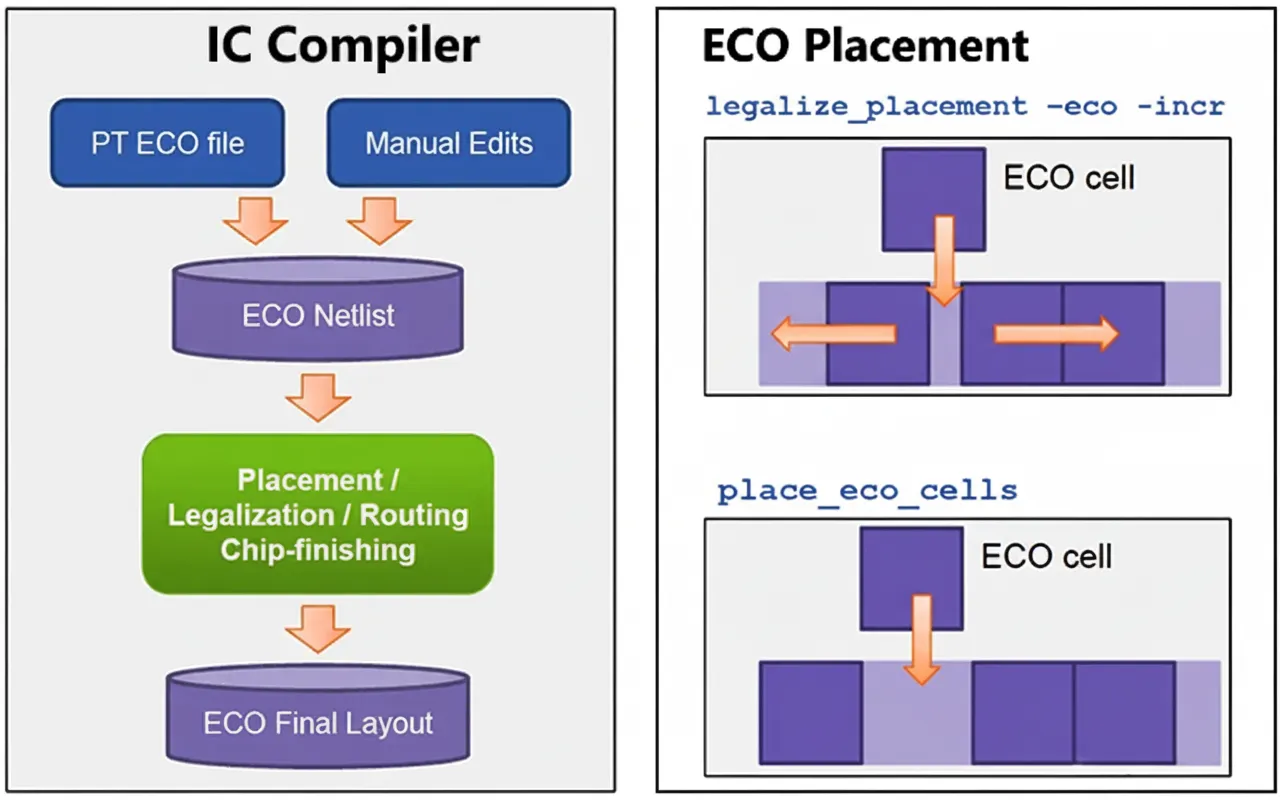
If an MPW or Full Mask prototype shows functional or performance defects, ECOs can make localized adjustments to routing and standard-cell placement to preserve the original layout as much as possible while fixing remaining violations. When backend place-and-route cannot fix violations without re-running the entire flow, ECOs are used to optimize timing, DRC, LVS, and power to meet sign-off criteria.
4. Tapeout corners
- Manufacturing is a physical process with process variation (doping concentrations, diffusion depths, etch depth, etc.). Variations occur between lots, between wafers in a lot, and across a single wafer.
- Different points on a wafer will not have identical carrier drift velocities. Device characteristics vary with voltage and temperature. These variations are captured by PVT (Process, Voltage, Temperature). The process dimension is further categorized into corners: TT (typical N, typical P), FF (fast N, fast P), SS (slow N, slow P), FS (fast N, slow P), and SF (slow N, fast P). The first letter denotes NMOS, the second PMOS. NMOS and PMOS devices are fabricated independently, so one may be relatively faster while the other is slower, which produces the FF, SS, FS, and SF cases. Process-driven adjustments tune device speeds and set FF/SS grading. Typically most devices are at TT; the five corners within +/-3 sigma cover roughly 99.73% of expected variation, assuming a normal distribution.
- Corner verification during engineering wafer runs is important. Foundries may run key layers to adjust inline variation and may use backup wafers to ensure production wafers are on target, i.e., near TT. If the objective is only to produce a few samples, corner validation may be skipped. For production readiness, corner coverage is mandatory. Design-stage simulations must verify circuit operation across corners and temperature extremes to ensure acceptable yields in production.
- Corner split strategy: product specs typically define margins in sigma. For example, "2FF" means two sigma toward the fast direction, while "3SS" means three sigma toward the slow direction. Sigma mainly quantifies Vt variation; larger sigma indicates greater variation. Allowances beyond nominal spec lines account for on-line process fluctuations.
5. Tapeout costs and wafer pricing
Mask costs and wafer costs dominate tapeout expenses. For a 40 nm node, mask costs are roughly $800,000–$900,000 and wafer cost per piece is around $3,000–$4,000. Including IP integration, total cost can reach about 7–8 million CNY.
Typical tapeout cost estimates by node: 28 nm about $2 million per run; 14 nm about $5 million; 7 nm about $15 million; 5 nm about $47.25 million; 3 nm may exceed $100 million. Mask sets are the largest single cost in mask-plus-wafer expenses.
More advanced nodes require more mask layers. Each mask layer corresponds to a photoresist coat, exposure, development, and etch step, incurring material and tool depreciation costs that ultimately are borne by the fabless customer.
Rough mask counts: 28 nm around 40 masks; 14 nm around 60 masks; 7 nm 80 or more masks. If one mask layer costs roughly $80,000, volumes are required to amortize costs.
Example, 40 nm MCU process: if producing 10 wafers, per-wafer cost = (900,000 + 4,000*10) / 10 = $94,000. If producing 10,000 wafers, per-wafer cost = (900,000 + 4,000*10,000) / 10,000 = $4,090. Greater wafer volumes reduce per-wafer cost, and vendor quotes vary.
Related Reading: What Does Advanced-Process Chip Design Cost?
Conclusion
Key stages from design to finished chip include design, tapeout, packaging, and testing, but cost distribution varies: roughly engineering labor 20%, tapeout 40%, packaging 35%, and testing 5%.
Tapeout carries significant risk. Failure rates vary by team and chip type but often fall in the 15%–35% range. Some analog sensor companies, even with complete teams and clear concepts, required many iterations: one example took eight years and 18 tapeouts to validate an analog-sensor IP and deliver an ultra-low-power, near-sensor device.