ALLPCB


01 EMC Overview
Introduction to electromagnetic compatibility
Electromagnetic compatibility (EMC) is a specialized but important field that spans many technical domains; it is effectively a discipline running through electronic technology.
Electromagnetic interference has become a major obstacle and bottleneck in the development of microelectronics, digital circuits, and analog circuit technologies.
Basic concept of electromagnetic compatibility
EMC refers to the ability of electrical and electronic equipment, in a given electromagnetic environment, not to emit excessive electronic noise to the outside while also being able to withstand a certain level of external electromagnetic interference.
In the 1990s the European Union first implemented mandatory EMC certification for electrical and electronic products entering its region, known as CE marking. Other regions followed with their own standards, such as the US FCC, Japan VCCI, and China's 3C.
Within EMC performance, the ability of electronic products to withstand transient strong disturbances such as lightning and electrostatic discharge is an important indicator of their immunity.
In short, circuit protection design is closely related to EMC performance; good protection design helps improve a product's EMC.
Scope:
- EMC covers frequencies up to about 400 GHz.
- For interference energy that damages equipment, most of it is concentrated at low frequencies; related data indicate about 90% is below 10 kHz.
- High-frequency interference tends to corrupt or distort signals.
Theoretical foundations of EMC
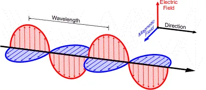
Basic units for electromagnetic interference field strength:
- Three units for high-frequency and microwave electromagnetic interference field strength:
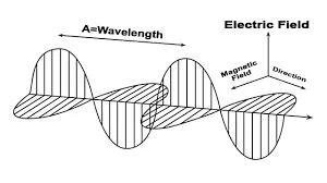
- Electric field strength: V/m
- Magnetic field strength: A/m
- Power flux density: W/m2
dB expresses the ratio between two quantities, commonly used to represent relationships that span large ranges. If P is the scene power level and P0 is the reference power level, the relationship is expressed in decibels.
Electromagnetic environment issues
Electromagnetic environment issues are of concern not only to electronic and electrical engineers but also to society and individuals. Electromagnetic environment problems are classified as natural interference and man-made interference.
Natural interference — electrostatics
Electrostatic discharge is one of the most common electromagnetic phenomena in nature. In dry regions, almost every person can carry more than 1.5 kV of static charge.
Static electricity arises from molecules and atoms; atoms consist of negatively charged electrons and positively charged protons.
Natural interference — lightning
Thunderstorms typically develop along frontal zones hundreds of kilometers long and 20–60 km wide. Fronts can move at 50–60 km/h, and can reach up to 100 km/h.
Natural interference — natural radiation
Man-made interference — radiated interference
Man-made radiated interference refers to interference propagated as electromagnetic waves from human activities:
- A region within about one wavelength of a source is the near field, where the source is central.
- A radius beyond one wavelength is considered the radiating (far) field.
- Near-field concept: from shortwave 30 MHz to microwave 30 GHz, wavelengths are roughly 0.01–10 m.
- Common radiated interference sources: transmitters, local oscillators, and nonlinear devices.
Man-made interference — conducted interference
Conducted interference sources:
- Electromagnetic noise from vacuums, switching devices, power switches, vehicle interference, circuit breaker contacts, radar transmitter ground loops, and similar sources.
Characteristics of conducted interference:
- Conducted interference frequencies are often considered under 100 MHz, although they can reach GHz.
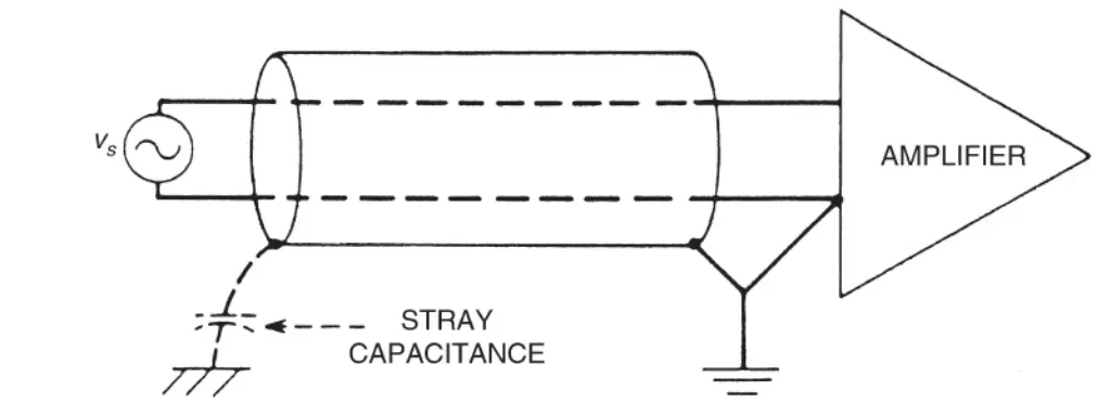
- High-frequency conducted interference is often neglected because conductor losses and wiring inductance and distributed capacitance cause significant attenuation of conducted power at very high frequencies.
02 EMC Testing
2.1 Electrostatic discharge (ESD) testing
ESD test standard reference: GB/T 17626.2 (IEC 61000-4-2).
Two modes
- Contact discharge: discharge gun with a pointed tip.
- Air discharge: discharge gun with a rounded tip.
Test equipment and discharge current waveform
Test requirements
- 150 pF capacitor represents the human body's energy storage capacitance.
- 330 Ω resistor represents the human body's internal resistance when holding a tool.
- Waveform rise time 0.7–1 ns, harmonic components include up to about 500 MHz.
- Discharge rate is 1 discharge/sec (sometimes 1 every 5 seconds).
- Typically discharge at selected points 20 times (10 positive and 10 negative).
- To ensure repeatability and comparability, the discharge electrode should be perpendicular to the surface of the equipment under test.
Notes:
- For coaxial and multi-core connector contacts: considering they have a metal connector shell, contact discharge is applied only to the connector's metal shell.
- For nonconductive enclosures (plastic, ceramic), where connector contacts are exposed, use air discharge with a rounded tip for evaluation.
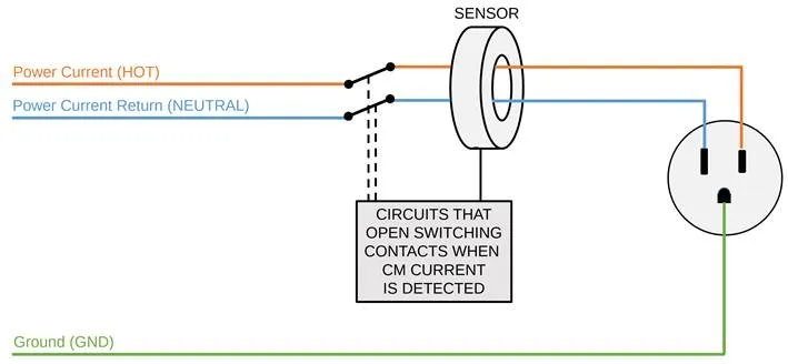
- Ungrounded equipment cannot dissipate charge before ESD is applied; it may hold up to twice the charge or voltage.
- For ungrounded equipment, extend the time between two tests to allow the previous charge to decay; use discharge resistors on grounding leads (two 470 kΩ) with a carbon fiber brush for discharge; using an ionizer for air neutralization is more complex.
2.2 Electrical fast transient/burst (EFT) testing
EFT standard reference: EFT GB/T 17626.4 (IEC 61000-4-4)
Modes and characteristics:
Burst pulses generally occur on power networks when many mechanical switches switch (interrupting inductive loads, relay contact bounce, etc.), producing interference.
Characteristics of EFT bursts:
- Burst group interval: 300 ms.
- Single pulse width: 50 ns ±30%.
- Pulse amplitude: 2 kV.
- Pulse rise time: 5 ns ±30%.
- Pulse repetition rate: 2.5 kHz ±20%.
- Positive and negative burst disturbance duration: 1 minute each.
Test equipment and discharge current waveform
Test requirements
Coupling/decoupling network characteristics and parameters as follows:
- Coupling capacitance: 33 nF.
- Coupling mode: common-mode.
- Capacitive coupling clamp.
- The distance between the coupling section and any other conductive section (excluding the cable under test and the reference ground plane) should be greater than 0.5 m.
- Typical coupling capacitance between cable and coupling clamp: 100–1000 pF.
- Usable diameter range for round cables: 4–40 mm.
- Insulation withstand voltage: 5 kV (using a combined wave of 1.2/50 μs).
- For acceptance tests on input/output and communication ports, use a capacitive coupling clamp.
- Interference generated by switching inductive loads or relay contact bounce affects ports (power, signal, control) in common-mode or differential-mode and can cause severe damage to operating systems.
- EFT/GB triple-standard requirements:
- Power and analog ports:
- Common-mode immunity: peak 2 kV, waveform repetition frequency 5 kHz.
- Differential-mode immunity: peak 1 kV, waveform repetition frequency 5 kHz.
- I/O signal/data and control ports:
- Common-mode immunity: peak 1 kV, waveform repetition frequency 5 kHz.
- Differential-mode immunity: peak 0.5 kV, waveform repetition frequency 5 kHz.
2.3 Surge testing
Surge immunity test reference: GB/T 17626.5 (IEC 61000-4-5).
Modes and characteristics
Requirements for combined waveform basic performance:
- Open-circuit output waveform conforms to 1.2/50 μs.
- Generator internal resistance: 2 Ω ±10%.
- Should form 12 Ω and 42 Ω resistive networks.
- Surge polarity: positive and negative.
- Phase: 0–360 degrees.
Requirements for communication line combined waveform:
- Open-circuit output waveform conforms to 10/700 μs.
- Generator dynamic internal resistance: 4 Ω.
- Surge polarity: positive and negative.
2.4 Immunity to induced RF fields
Conducted RF disturbance induced onto cables: GB/T 17626.6 (IEC 61000-4-6).
Test requirements
Standard radiated immunity tests are performed on a compliant open test site where an RF transmitter generates a spatial electromagnetic field. These fields induce currents or voltages on the device under test's connected cabling, affecting the equipment.
Test level: frequency range 150 kHz–80 MHz (can be extended to 230 MHz).
This covers magnetic fields from medium-wave, short-wave, FM broadcast, and TV transmitters.
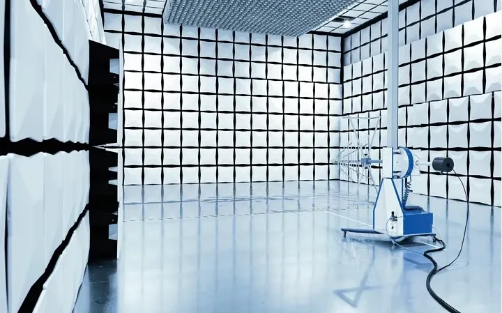
2.5 Anechoic chamber testing
Anechoic chamber: EN 55022 / EN 61000-4-3. Chambers are classified as semi-anechoic and fully anechoic.
Semi-anechoic chamber
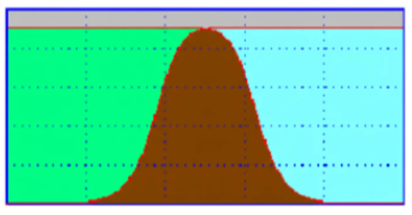
The field received by the antenna is the vector sum of the direct wave and reflected waves, with their phase relationship affecting the resultant field. Maximum field strength occurs when the path difference between reflected and direct waves is an integer multiple of the free-space wavelength so that the phases add.
Fully anechoic chamber
A fully anechoic chamber differs by not receiving reflections from the planar ground; ideally the propagation characteristics should match those of free space.