 ALLPCB


In the world of printed circuit board (PCB) design, vias play a critical role in connecting different layers of a board. However, improper placement—especially cumulative or excessive clustering of vias—can lead to serious issues like electromagnetic interference (EMI), degraded signal integrity, and plane voids in power or ground layers. So, how can you avoid the cumulative placement of vias in PCB designs? The key lies in strategic planning, understanding the impact of via placement on EMI and signal integrity, and adhering to best practices for multilayer designs. In this comprehensive guide, we'll dive deep into the importance of avoiding via clustering, explore its effects on PCB performance, and provide actionable tips to optimize your designs for better reliability and efficiency.
Understanding Vias in PCB Design
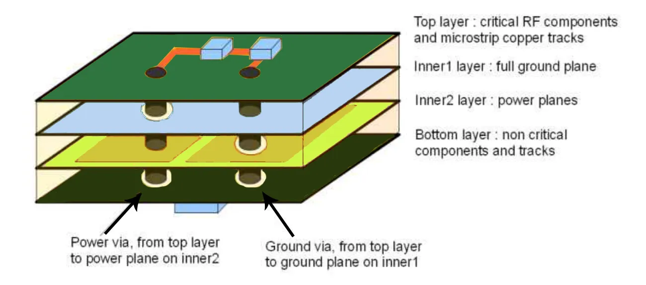
Vias are small conductive holes in a PCB that allow electrical connections between different layers. They are essential for routing signals, power, and ground connections in multilayer boards. However, when vias are placed too close together or in large clusters—known as cumulative placement—they can create unintended problems. These issues include increased EMI, signal integrity degradation, and disruptions in power and ground planes, often referred to as plane voids.
Before we explore solutions, let’s break down why cumulative via placement is a concern. When vias are densely packed, they can act as unintended antennas, radiating electromagnetic noise. This noise interferes with nearby signals, causing data errors or timing issues in high-speed designs. Additionally, excessive vias in power or ground planes can create gaps or voids, disrupting the uniform flow of current and increasing impedance. For engineers working on high-frequency or high-speed circuits, these problems can be catastrophic.
Why Cumulative Via Placement Harms PCB Performance
Cumulative placement of vias can have a ripple effect on the overall performance of a PCB. Below, we’ll explore the specific ways it impacts EMI, signal integrity, and power plane integrity, supported by practical insights and data.
1. Increased Electromagnetic Interference (EMI)
When vias are placed too close together, especially in high-frequency designs, they can couple with each other, creating parasitic inductance and capacitance. This coupling leads to EMI, where unwanted electromagnetic noise radiates from the board and interferes with nearby components or external devices. For instance, in a design operating at frequencies above 1 GHz, closely spaced vias can increase radiated emissions by up to 20-30% compared to properly spaced vias, based on typical industry simulations.
EMI not only affects the performance of your PCB but can also cause compliance issues with regulatory standards like FCC or CE. Avoiding cumulative via placement is crucial to minimize these risks and ensure your design meets electromagnetic compatibility (EMC) requirements.
2. Degraded Signal Integrity
Signal integrity refers to the quality of an electrical signal as it travels through the PCB. Cumulative via placement can introduce impedance mismatches and crosstalk, leading to signal distortion. For high-speed signals, such as those in DDR4 memory operating at 3.2 Gbps, even a small cluster of vias can cause reflections, increasing bit error rates by as much as 10^-6 or more, depending on the design.
Vias also add inductance to the signal path. When multiple vias are placed in close proximity, this inductance accumulates, further degrading signal quality. Proper spacing and strategic placement are essential to maintain clean, reliable signals, especially in modern high-speed applications.
3. Plane Voids in Power and Ground Layers
In multilayer PCBs, power and ground planes provide a stable reference for signals and ensure low-impedance paths for current. However, placing too many vias in these planes can create voids or gaps, disrupting the continuity of the plane. These plane voids increase the loop inductance, leading to voltage drops and noise in the power delivery network (PDN). For example, a void caused by a cluster of vias in a ground plane can raise the impedance by 50% or more in affected areas, based on typical PDN analysis.
Plane voids also affect thermal management, as they reduce the copper area available for heat dissipation. For designs with high current demands, this can lead to overheating and long-term reliability issues.
Best Practices for Avoiding Cumulative Via Placement
Now that we understand the risks associated with cumulative via placement, let’s explore actionable strategies to avoid it. These best practices will help you optimize your PCB design for minimal EMI, improved signal integrity, and robust power and ground layers.
1. Plan Via Placement During the Schematic Stage
The first step to avoiding cumulative via placement is to plan your design early. During the schematic stage, identify critical signal paths and power delivery requirements. Use this information to estimate where vias will be needed and avoid overusing them in specific areas. For instance, group signals that require layer transitions in a way that minimizes via density, and consider alternative routing strategies to reduce the total number of vias.
Modern design tools often include features for via planning and optimization. Leverage these tools to simulate via placement and identify potential clustering issues before moving to layout.
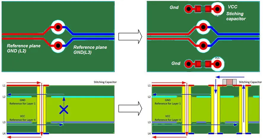
2. Use Via Stitching Sparingly and Strategically
Via stitching is a technique used to connect ground planes across layers, often to reduce EMI and improve signal return paths. However, excessive via stitching can lead to cumulative placement and plane voids. To avoid this, place stitching vias only where they are needed, such as around high-frequency components or along the edges of the board. A common guideline is to space stitching vias at a distance of λ/20, where λ is the wavelength of the highest operating frequency. For a 2.4 GHz signal, this translates to a spacing of about 6 mm.
Additionally, ensure that stitching vias are evenly distributed rather than clustered in one area. This approach maintains ground plane integrity without creating unnecessary voids.
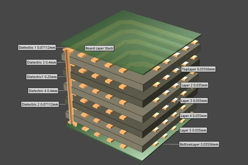
3. Optimize Layer Stackup to Minimize Via Usage
A well-designed layer stackup can significantly reduce the need for vias. For example, dedicate specific layers to high-speed signals and route them to avoid frequent layer transitions. In a 6-layer PCB, you might assign layers 1 and 6 for signal routing, layers 2 and 5 for ground, and layers 3 and 4 for power. This stackup minimizes the need for vias by keeping critical signals on outer layers and providing direct access to reference planes.
By reducing layer transitions, you inherently lower the number of vias required, making it easier to avoid cumulative placement. If transitions are unavoidable, stagger vias across different areas of the board to prevent clustering.
4. Maintain Proper Spacing Between Vias
Spacing is critical when it comes to via placement. As a general rule, maintain a minimum spacing of at least 3 times the via diameter between adjacent vias to reduce coupling and parasitic effects. For example, if your via diameter is 0.3 mm, ensure a spacing of at least 0.9 mm. This spacing helps minimize EMI and prevents the formation of plane voids in power and ground layers.
For high-density designs where spacing is constrained, consider using microvias or blind vias, which have smaller diameters and can be placed closer together without significant impact on performance. However, always balance density with manufacturability and cost considerations.
5. Simulate and Analyze Via Placement for EMI and Signal Integrity
Before finalizing your design, use simulation tools to analyze the impact of via placement on EMI and signal integrity. Tools like signal integrity simulators can model the effects of via clustering on impedance, crosstalk, and reflections. For instance, a simulation might reveal that a cluster of vias near a high-speed signal line increases return loss by 10 dB at 5 GHz, prompting you to adjust the layout.
Similarly, EMI simulation software can help identify areas of high electromagnetic radiation caused by via placement. Use these insights to redistribute vias and optimize your design for better performance.
Advanced Techniques for High-Speed PCB Designs
For engineers working on high-speed or high-frequency PCB designs, avoiding cumulative via placement requires additional considerations. Here are a few advanced techniques to further enhance your design process.
1. Implement Back-Drilling for Stub Reduction
In high-speed designs, vias often create stubs—unused portions of the via barrel that act as resonant structures, causing signal reflections. Cumulative via placement exacerbates this issue. Back-drilling, a process that removes these stubs by drilling out unused via sections, can mitigate reflections and improve signal integrity. While back-drilling adds to manufacturing costs, it’s a valuable technique for designs operating above 10 Gbps.
2. Use Differential Pair Routing with Controlled Vias
For differential signals, such as those in USB 3.0 or PCIe, ensure that vias for each pair are placed symmetrically and with controlled spacing. Cumulative placement can disrupt the differential impedance, typically around 100 ohms for many high-speed standards, leading to signal skew and data errors. Route differential pairs on the same layer whenever possible, and if vias are needed, keep them minimal and balanced.
Common Mistakes to Avoid in Via Placement
Even with the best intentions, it’s easy to make mistakes in via placement. Here are a few common pitfalls and how to avoid them:
- Overusing Vias for Convenience: Don’t add vias just because they make routing easier. Each via should serve a specific purpose, and unnecessary vias should be eliminated during design reviews.
- Ignoring Return Paths: Vias can disrupt signal return paths, especially when clustered near critical traces. Always ensure a continuous return path by placing ground vias strategically.
- Neglecting Thermal Effects: Cumulative via placement in power planes can create hotspots due to reduced copper area. Use thermal simulation to identify and address potential overheating issues.
Conclusion: Designing Smarter PCBs with Optimized Via Placement
Avoiding the cumulative placement of vias in PCB designs is a fundamental step toward achieving reliable, high-performance circuits. By understanding the risks of EMI, signal integrity degradation, and plane voids, and by following best practices like strategic via spacing, layer stackup optimization, and simulation-driven design, you can create PCBs that meet the demands of modern electronics. Whether you’re working on a simple 2-layer board or a complex high-speed design, thoughtful via placement will ensure better power delivery, cleaner signals, and compliance with industry standards.
Start implementing these strategies in your next project to see the difference in performance and reliability. With careful planning and the right tools, you can master the art of via placement and take your PCB designs to the next level.


